Silicon Co-Design

Silicon Co-Design

High Speed Optical / Wireline Communications

A Comprehensive Deep Dive into High-Speed HBM5 Interconnect: Signal Integrity and Co-Design Challenges

How transmission line effects and power-supply induced jitter make high-speed HBM interconnect scaling one of the most challenging co-design issues in AI racks

Chad's avatar
Chad
Jul 15, 2026
∙ Paid

While a lot of attention is being drawn to the current HBM4 shortage, this post will focused on the practical technical challenges in scaling HBM5 performance.

I will discuss the following signal integrity and co-design challenges in HBM5 based on SK Hynix and KAIST’s ECTC 2026 papers:

  • Introduction to Signal Integrity trends from HBM1 to HBM5

  • Jitter component tree and descriptions of key sources of jitter for short, high-speed interconnect:

    • Echo

    • SSC / SSN

    • PSIJ

  • How SK Hynix quantifies transmission line effects in high-speed HBM5 data lines

    • Fundamentals of Transmission Lines

    • Proposal for two operating regions: RC and LC dominated regimes

    • 🔒Design of Experiments results for echo jitter across interconnect lengths and dimensions

  • 🔒KAISTs SI/PI co-analysis framework for Chiplet (UCIe)-based GPU-HBM Interconnect for PSIJ

    • 🔒Shoreline density limitations for a 4 layer wide-IO and chiplet interconnect scheme

    • 🔒Calculating power-supply induced jitter (PSIJ) from SI, PI, SSC, and jitter sensitivity / amplification

  • 🔒BONUS: “The Brain” - 3D Custom HBM and current status among TSMC, SK Hynix, NVIDIA, and Samsung from ECTC 2026

This post is heavily influenced by the ECTC session 11, “Signal Integrity Design for High-Speed Interfaces” as well as my experience at DesignCon 2026 I was personally in attendance for.

This will be more of an advanced deep dive, but grounded in fundamentals. I structured the post to start with baseline EE concepts and building a framework to understand the complexity of multi-layer SI/PI co-design. I have a post that covers the fundamentals of signal integrity that forms the foundation of the issues I discuss:

High-Speed Signal Integrity: Physical Impairments and Equalization Architectures

High-Speed Signal Integrity: Physical Impairments and Equalization Architectures

Chad
·
Mar 17
Read full story

I encourage you to read through my backlog of knowledge and challenge you to take away one new in-depth concept. Even if the technical material doesn’t stick, I still hope you come away with an appreciation of the challenges that keep HBM and SI engineers up at night.

Note that I am not a signal integrity person. However, I immersed myself into the SI world by attending DesignCon 2026 with an RF / Microwave lens upon which to analyze high-speed signal integrity effects. It was clear upon reading these papers that memory and SI engineers do not speak the same language as RF people do, but they describe the same effects from their point of view.

I personally think that at increasingly faster data rates, there will be a convergence of the knowledge among RF / microwave and signal integrity domains. I aim to bridge this gap of understanding.

Silicon Co-Design is a reader-supported publication. To receive new posts and support my work, consider becoming a free or paid subscriber.

SK Hynix - High speed HBM roadmaps

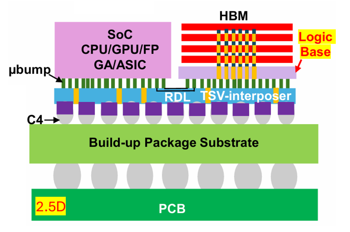
Figure 1. HBM used in 2.5D Packaging. Source: J. Lau. “Advanced Packaging for Chiplets, Heterogeneous Integration, and Co-Packaging Optics” ECTC2026

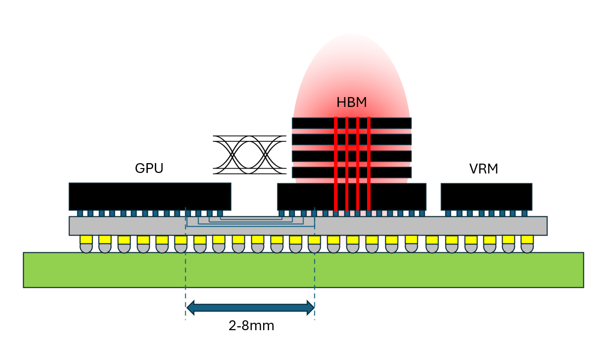
High bandwidth memory (HBM) is a critical component for AI training workloads that stores everything involved in AI computation from model weights, gradients, optimizer states, and activations. HBM connects multiple DRAM dies vertically using TSVs to maximize memory density in the given footprint. These DRAM dies are placed as close to the GPU as possible to maximize the data throughput to overcome the Von-Neumann bottleneck.
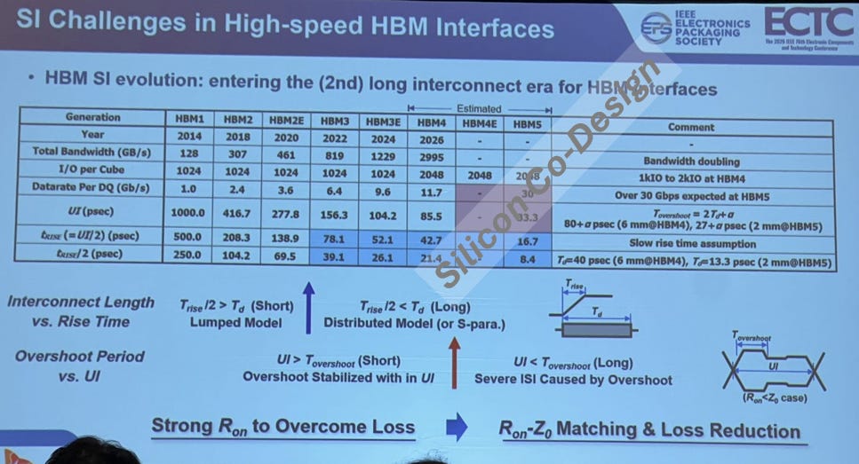
Figure 2. SI Characteristics in Scaling HBM from Gen 1 to Gen 5. Source: T. Bae et al. “Figures of Merit to Characterize the Signal Integrity Performance of Interposer Interconnect for High Bandwidth Memory (HBM)” ECTC2026

In this SK Hynix roadmap presented at ECTC 2026, there are a few performance scaling trends along HBM generations:

  • Between HBM1 and HBM4, the datarate per DQ increased linearly from 1Gb/s to 11.7Gb/s

  • Along those generations, the signal rise time and unit interval (UI) scaled inversely proportional to the total data rate per DQ

  • Between HBM3E and HBM4, there is a stairstep jump in the the total bandwidth by 2.5x, primarily driven by doubling I/O per cube from 1024 to 2048.

To keep with up AI workload demands, HBM5 expects a 20-30 Gbps per DQ range using state-of-the art interposer technologies such as the Chip-on-Wafer-on Substrate (CoWoS-L and CoWoS-R).

At those data rates, HBM is running into co-design challenges along the signal integrity, power integrity, and thermal domains. At ECTC, there are three high-level trends I noticed amongst three papers:

Jitter due to Transmission Line Effects
SK Hynix notes that significant transmission line effects were not observed for previous HBM generations with a data rate of under 10 Gbps per DQ and approximately 6-mm-long interposer interconnects.

However, at 30Gbps rates, advanced packaging interconnect technologies exhibit distinct lossy transmission line characteristics and must be accounted for.

Normally, transmission lines are terminated with equivalent impedances to avoid reflections. However, termination resistors cannot be reasonably employed for terminating 1000+ I/O in HBM as this would lead to high thermal penalties and static power dissipation. This leads to additional signal integrity challenges that will be discussed.

From “Wide-and-slow” to UCIe
Another challenge is edge density limitations of I/O. Doubling the number of I/O pins results in excessively large physical layer (PHY) footprint on the silicon. The number I/O is fundamentally constrained by the metal pitch, # of layers, and the area dedicated to ground rails to control crosstalk.
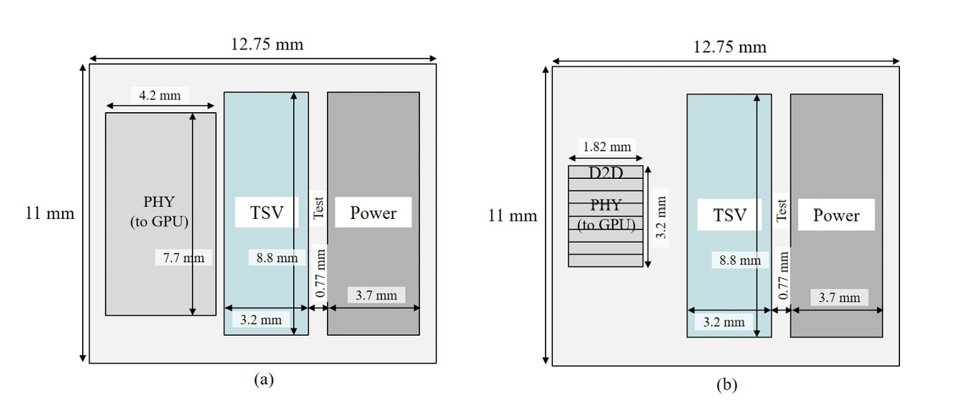
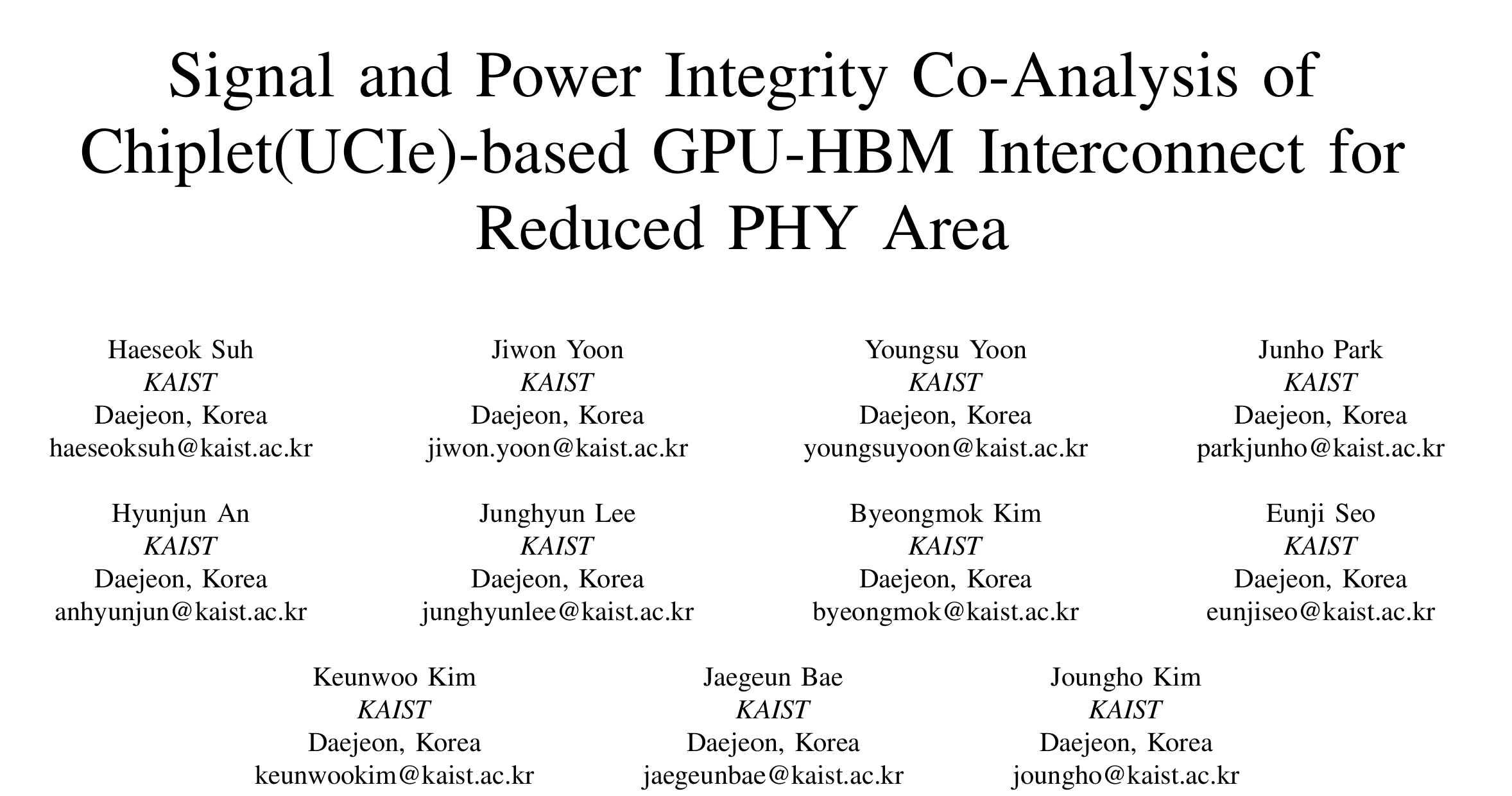
Figure 3. An illustration of the shoreline for HBM4 with conventional (and G2D module. Source: H. Suh. “Signal and Power Integrity Co-Analysis of Chiplet(UCIe)-based GPU-HBM Interconnect for Reduced PHY Area” ECTC2026

To scale the number of I/O, KAIST is investigating the performance impact of going from wide-and-slow I/O toward higher-speed SerDes lanes in Universal Chiplet Express (UCIe) standards.

KAIST notes that in chiplet-based GPU-HBM based on UCIe, eight D2D modules are utilized, with each module consisting of 64 Tx and Rx at 32Gb/s each. A total of 512 Tx and Rx supports 2 TB/s for read and write directions.

With a faster, more compact PHY, more I/O them can fit in the HBM shoreline to increase the data throughput.

PDN for 3D stack
Another co-design challenge is how the TSVs in the HBM stack affect thermal characteristics.
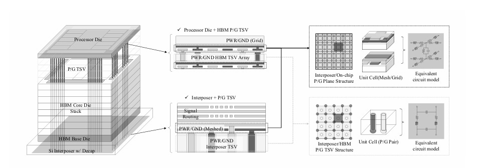
Figure 4. An Illustration of TSVs and the power grid structure used. Source: J. Yoon et al. “Power Distribution Network (PDN) Design and Analysis for Multi-Stack 3D Heterogeneous Integrated High Bandwidth Memory (3D-HI-HBM) Module” ECTC2026

This paper evaluates the thermal and IR drop characteristics of different TSV configurations. Here we see how each component is modelled as an array of unit cells in a grid structure with an equivalent RLC circuit model.

Though I think this paper is important for effective co-design, especially when it comes to modelling PDNs for PSIJ, I have left the analysis out of this post for now to focus on signal integrity challenges from the first two papers.

Silicon Co-Design is a reader-supported publication. To receive new posts and support my work, consider becoming a free or paid subscriber.

Key sources of jitter in high-speed, low-voltage parallel lines

Figure 5. A eye measurement for HBM showing aperture and jitter. Source: T. Bae et al. “Figures of Merit to Characterize the Signal Integrity Performance of Interposer Interconnect for High Bandwidth Memory (HBM)” ECTC2026

Jitter is a key constraint of high speed signal integrity and must be accounted and minimized as much as possible.

When high speed data is sent to and from the HBM, each bit is received within a given time slot refers to as the “Unit Interval” (UI) or Bit-period. Jitter and slew rate constraints reduce this to an effective aperture “window” where data can be received. Throughout the post, all aperture results are normalized to a UI of 1.

Figure 6. Jitter component tree showing both the statistical effects of jitter and the physical mechanics that cause them. Source: M. Li. “Design and Verification for High-Speed I/Os at 10 to 112 to 224 Gbps, and 448 Gbps with Jitter, Signal Integrity, and Power Optimized” DesignCon 2026

There are many difference sources of jitter as shown in this comprehensive jitter tree from Dr. Mike Peng Li’s DesignCon 2026 tutorial slides.

Jitter is broken down into two main statistical categories: deterministic and random jitter. I describe these in more detail, along with equalization techniques, in the following post:

High-Speed Signal Integrity: Physical Impairments and Equalization Architectures

High-Speed Signal Integrity: Physical Impairments and Equalization Architectures

Chad
·
Mar 17
Read full story

Under deterministic jitter, there are three primary classes of jitter relevant to high speed, massively parallel, non-terminated lines:

  • Echo Jitter - Jitter caused by impedance mismatches and reflections

    • When a signal propagates down the line and encounters an impedance mismatch, part of the signal reflects backward and forwards, resulting in a stored “memory” and overshoot that affects future bit measurements. This can lead to ISI.

  • Bounded Uncorrelated Jitter - Jitter that is bound but uncorrelated to the signal

    • This includes crosstalk across massively parallel lines where there are many different possible combinations of crosstalk interactions, but the overall jitter impact is “bounded” to worst case conditions.

  • Periodic Jitter - Jitter where the timing variations repeat in a cyclical pattern over time at a specific frequency

    • This includes simultaneous switching noise that occurs every switching period.

Figure 7. A high level illustration of PSIJ manifesting from power noise from the VRM coupling. Source: H. An et al. “Analytical Approach to Statistical Modeling of Power Supply Induced Jitter” ECTC2026

One source of jitter that is particularly problematic at increasing data rates is power-supply induced jitter (PSIJ) which is a form of power-noise-induced timing degradation within circuits themselves. This is a challenge to model because it combines jitter from a few sources.

The rise / fall time and propagation delay of a circuit depends on how quickly FET caps can get charged by the PDN. When gates are switched, they generate simultaneous switching current (SSC) that go through the PDN and cause simultaneous switching noise (SSN) on the line. Noise on the PDN can affect the current your caps charge at, introducing timing uncertainty.

PSIJ becomes more problematic as you stack and cram more HBM on the same PDN and the PDN line becomes noisier. With increasing data rate, thousands of I/O drivers switching simultaneously, and a low supply voltage, a marginal increase in PSIJ can eat into the jitter budget and lead to signal failures. A co-design approach to modelling PSIJ will be discussed in more detail behind the paywall.

Silicon Co-Design is a reader-supported publication. To receive new posts and support my work, consider becoming a free or paid subscriber.

How SK Hynix must incorporate transmission line effects in high speed HBM data lines

Now lets discuss some of the high-speed SI challenges SK Hynix is facing from transmission line effects. I’ll start with a broad introduction of transmission effects from an RF point of view, the nuances as it relates to SI, then jump right into SK Hynix’s analysis after the paywall.

From Lumped to Distributed Abstraction

Most circuit analysis (like V = IR) is initially taught in the “lumped” abstraction where component values are “lumped” or simplified into devices consisting of resistors, capacitors, and inductors. Lumped abstractions form the basis of most traditional circuit analyses like nodal, mesh, etc.

The important thing about a lumped abstraction is that the propagation characteristics of the physical connections between lumped components can be reasonably neglected for most practical applications if the frequency is low enough.
When the frequency is low enough, the signal level will be virtually the same across all lengths of the wire since the capacitors distributed throughout the line charge nearly instantaneously.

Figure 8. The instantaneous voltage across a transmission line whose length is an appreciable percentage of the total wavelength. Source: T. Bae. “Figures of Merit to Characterize the Signal Integrity Performance of Interposer Interconnect for High Bandwidth Memory (HBM)” ECTC 2026

However, at high frequencies, the signals have to physically propagate down the wires to get from point A to B, so the physical characteristics of the interconnects are important. This is referred to as the “distributed” abstraction where the electromagnetic wave propagation characteristics along a transmission line matter. Notice how in the figure above, when a high frequency wave is sent down a line, its voltage rises at different time points.

When deciding on whether to model circuits with lumped or distributed elements, the rule of thumb I was taught in RF classes is that:

Transmission line effects start taking effect when the line length is approximately 10% of the signal wavelength.

For interconnects that are approximately 6mm and an er of 4, this corresponds to a frequency of 2.5 GHz. Its clear that HBM data rates are running into this regime.

Figure 9. A Signal characteristic of a transmission line. A signal is launched down the line and reached the open termination end in a time delay Td. This signal is then “reflected” back toward the source where it then encounters an impedance mismatch between Ron = 14 ohm and Zo = 35 ohms, and is then reflected back toward the end two Td’s later to lower the voltage. Capacitive loads affect the rise / fall time characteristics. Source: T. Bae. “Figures of Merit to Characterize the Signal Integrity Performance of Interposer Interconnect for High Bandwidth Memory (HBM)” ECTC 2026

In transmission line theory, when a wave is sent down a line with a characteristic impedance Zo, there needs to be an equal impedance at the termination for the signal to “match” to, or else the wave will reflect backwards. The reflection coefficient quantifies this effect and its formula is given by:

When the impedance is NOT matched, the reflection coefficient is not 0. Depending on the extend of impedance mismatch, a portion of the wave that makes it way to the load is then reflected backwards and forwards along the line in a time delay T_d, decaying over time.

For an open ended or high impedance circuit, Z_L is infinite and the reflection coefficient is 1. This means that for high frequency RF signals, all of the propagated signal gets sent backwards as there is nowhere it can terminate. This is shown as the “stairstep” function in figure 8.

Figure 10. Smith Source showing an impedance transformation of a quarter wavelength line. (Note that Smith Chart analysis is not always valid for high speed digital signals, but is a useful tool to build intuition on the effects) Source: By Cannabic - Own work, CC BY-SA 4.0, https://commons.wikimedia.org/w/index.php?curid=112020975

From the source POV, the effective impedance looking into the line depends on the length of the line between the source and termination. An impedance on a smith chart can be rotated depending on the integer multiple of wavelengths to find the equivalent impedance “looking” into the line. A special case (commonly asked in interviews) is λ / 4 lines that “transform” a open ended impedance to a short circuit looking into the line.

Though RF has a highly developed body of broadband analysis techniques such as smith charts, there are a few caveats as it applies to signal integrity:

  • The data is digital data are ideally square waves with rise/fall times and odd mode harmonics, not broadband sine waves. When a signal goes high at the source, its value stays high at a fixed level until the next time period.

  • The interconnect resistance is fairly high (1’s to 10’s of ohms) compared to the characteristic impedance. In most lossy RF transmission lines with enough board space, the resistance will usually not be this high. The only reason its high for HBM is for the tiny wires they need for the massive parallelism.

  • In RF theory, the characteristic impedance is commonly standardized to 50 ohms and the source impedance matches this. However, matching the source impedance to the HBM interconnect impedance is not practical because changing Ron can fix one problem but create others:

    • Increasing Ron to impedance match will cut the launched voltage is half and charge the line slower, decreasing slew rate

    • Decreasing Ron would require large width transistors that may cut into edge density

    • Therefore, SK Hynix selects a Ron of 14 ohms for a characteristic impedance of 34 ohm to balance the tradeoffs of layout area and slew rate. This results in a reflection coefficient of -0.41 at the source end.

In short, for 30Gb/s data rate per DQ HBM5, SK Hynix is dealing with a tricky combination of high channel resistance and transmission line effects that can’t be easily analyzed using standard microwave techniques, and thus have to define their own set of evaluation criteria for high speed signal integrity. These evaluation criteria involve classifying the mode the operation into two distinct regions:

  • RC Dominated

  • LC Dominated

Silicon Co-Design is a reader-supported publication. To receive new posts and support my work, consider becoming a free or paid subscriber.

Share

After the paywall I will discuss this methodology along with KAISTs co-design framework in more depth. In the meantime, checkout a few of my other posts.

Solving AI’s Beachfront Crisis for 200Gbps+ Interconnect: Marvell & Celestial AI’s Optical Answer to Nvidia’s NVLink

Solving AI’s Beachfront Crisis for 200Gbps+ Interconnect: Marvell & Celestial AI’s Optical Answer to Nvidia’s NVLink

Chad
·
Jul 8
Read full story
Pushing the Speed Limit: Designing SerDes Transceivers for the 224 and 448Gbps Scaling Era

Pushing the Speed Limit: Designing SerDes Transceivers for the 224 and 448Gbps Scaling Era

Chad
·
Mar 23
Read full story
High-Speed Signal Integrity: Physical Impairments and Equalization Architectures

High-Speed Signal Integrity: Physical Impairments and Equalization Architectures

Chad
·
Mar 17
Read full story

Side note: I saw a crazy idea at ISSCC 2026 where the data between GPU and HBM was…

This post is for paid subscribers

Already a paid subscriber? Sign in
© 2026 Chad Wallace · Privacy ∙ Terms ∙ Collection notice
Start your SubstackGet the app
Substack is the home for great culture