
High-Speed Signal Integrity: Physical Impairments and Equalization Architectures
How signal integrity influences complexity of modern wireline transceiver architecture from first principles

Editor’s Note (6/1/26): Moving forward, I am transitioning this Substack into a deep-dive resource on System Architecture that covers the packaging, thermal, power, and signal integrity stack. To reflect the depth and combination of the synthesis, the deepest technical layers of my guides will now be reserved for paid subscribers.
In this post I cover the following topics:
SerDes - The Workhorse of chip to chip communication
The Root Causes of Signal-Integrity Degradation at High Speed
How Channel loss and Jitter degrade Bit Error Rate
Major System Trends:
PAM-4
DSP-based Architectures
🔒Error Reduction Techniques
🔒Forward Error Correction
🔒Equalization
🔒TX - Pre-emphasis / FFE
🔒RX - CTLE and DFE
🔒How to Achieve Higher Data Rate
Everyone talks about the importance of chip-to-chip communication, but few people appreciate the complexity hiding underneath it.
Signal integrity and SerDes architecture are often discussed as if they belong to different worlds: one in the lab and on the board, the other inside the chip. In reality, they are deeply coupled.
My goal in this post is to show how signal-integrity constraints at the channel and board level—loss, jitter—affect performance through BER and ultimately drive complexity back into the transceiver itself, shaping choices in equalization, clocking, and data conversion. Here I’ll focus on the signal-integrity foundations from first principles, then build on that in a follow-up post on chip architecture.
Much of the content of this post is material consolidated from a Tutorial given by Dr. Mike Peng Li from DesignCon 2026, the premier high-speed communications conference, as well as from ISSCC, academic papers and SI books. Figures are reproduced for commentary and educational purposes.
SerDes - The Workhorse of chip to chip communication
A serializer-deserializer (SerDes) converts parallel digital data into a high-speed serial stream for transmission, then reconstructs it at the receiver. This allows systems to move large amounts of data between chips and systems without requiring a huge number of parallel wires.
SerDes and optical links are the “workhorses” of communication within data centers in “scale up” and “scale out” networks:
Chip to chip
Modular top chip copper links on a PCN and an optical module
Between a CPU and network interface
Backplane and midplane links over backplane PCBs or passive copper cables
SerDes is what enables parallel computing across many CPUs and GPUs as a means of data distribution.
Historically, many SerDes architectures have been analog-based. SerDes speeds have scaled with PAM-2 (NRZ) signals over time to meet the growing needs of traditional computing.
Then, AI and chiplets came in and started demanding more data.
These two technological trends put a lot of pressure on chip-to-chip communication to get faster and reach farther due to the massive amounts of data movement:
AI workloads involve massive data movement: repeated memory access, movement of intermediate results, and parallel processing across many GPUs in a rack.
Chiplets disaggregate a system into multiple smaller dies, which must then be tied back together through high-speed chip-to-chip interfaces.
However, as data demands push speeds higher and links longer, fundamental physics begins constraining performance:
Channel loss due to higher attenuation at higher frequencies
Jitter budgets getting tighter
Transmission line effects that cause distortions
Noise that can cause errors
These add complexity to the SerDes to correct for. Unfortunately, the added complexity makes it more challenging to understand how one part of the system affects the other, such as:
How jitter in the VCO eats into the timing margin needed to meet the target BER
How receiver clock skew and TI-ADC area constraints affect sampling margin, data throughput, and calibration burden
In the following sections I’ll be focusing on signal integrity fundamentals from first principles. The goal is to ask:
What are the fundamental physics constraints limiting performance?
What complexity in the chip architecture is needed to scale speeds beyond 112.5Gbps to 224Gbps and eventually 448Gbps?
The Root Causes of Signal-Integrity Degradation at High Speed
In this section, I’ll focus on describing two primary causes of signal-integrity degradation at high speeds: channel loss, and jitter. I’ll then show how they affect BER.
Channel loss in Copper interconnects
Copper is widely used as the interconnect of choice to transmit signals between chips due to its high electrical conductivity and durability.
Copper has been used for many years at low data rates where the losses were much less. However, the loss increases at higher signal frequencies. There are two major loss mechanisms:
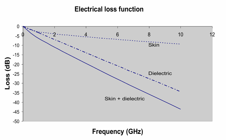
Dielectric loss. Dielectric loss occurs due to heat energy dissipation of dipoles at high frequencies. A quickly alternating electric field in the dielectric causes polarization in dipoles in the dielectric (i.e. the positive and negative parts of the atom move apart) and results in energy dissipation through heat.
Dielectric loss scales with frequency and is generally the dominant loss mechanism at the data rates that modern SerDes nowadays run at.
Skin effect. Skin effect occurs when time-varying electromagnetic fields push current toward the edges of the conductor. This results in an effective lowering of the cross-sectional area that the signal actually “sees”.
Skin-effect loss scales roughly with the square root of frequency and has historically been a major source of channel loss until dielectric loss becomes more dominant at higher frequencies.
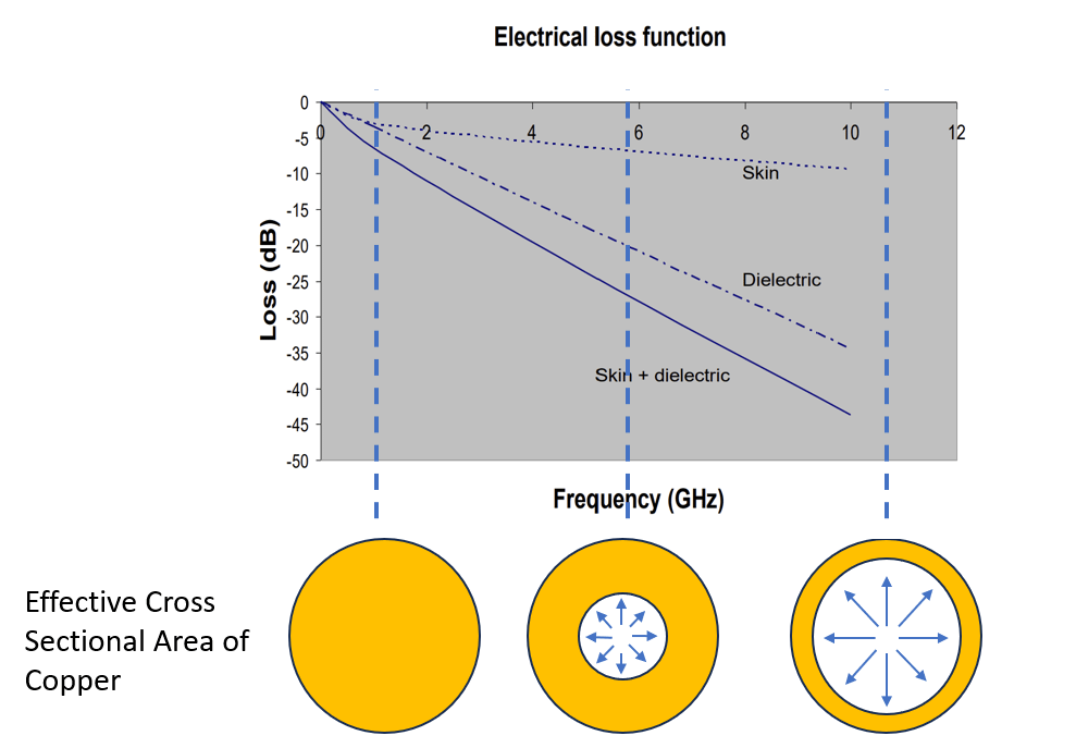
In both cases, signal attenuation increases with frequency. This means that signals with multiple frequency components like square waves will have higher order frequencies attenuated more strongly. This will result in a “rounding” of the signal at the other end with degraded amplitude.
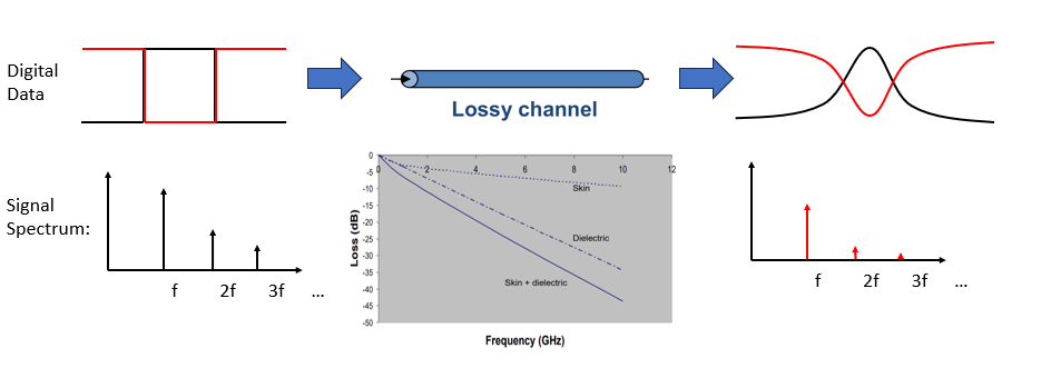
Modern 112G PAM4 systems typically target 25 dB to 35 dB of channel loss.
Jitter
Jitter is defined as the time variation in when a signal edge actually transitions compared to its ideal transition point. Jitter is a significant limiter of performance in high-speed applications because it affects how much of a time ”window” you have to accurately sample the digital data.
Jitter is broadly broken down into two major categories: Random and Deterministic:
Random Jitter comes from noise-like mechanisms that are fundamentally statistical in nature, such as thermal noise.
This is always uncorrelated and typically modelled as a Gaussian distribution due to the central limit theorem that states that summing up a variety of PDFs from uncorrelated sources tend toward a Gaussian distribution.
Deterministic Jitter is jitter from repeatable structure in the system such as data movement and reflections.
This jitter is typically bounded with a max and min timing shift - the edge shifts in a repeatable way. It can also be correlated or uncorrelated. Examples include:
Data dependent jitter (ISI) - Symbols from previous transitions spill into the next time window
Periodic Jitter
Bounded uncorrelated jitter
As link complexity has grown, many other jitter sources must be accounted for during design and measured in silicon.
How Channel loss and Jitter degrade Bit Error Rate
Both losses distort the signal in complementary ways:
Channel loss distorts the waveform itself by attenuating and smearing its higher-frequency content
Jitter introduces uncertainty in when transitions occur.
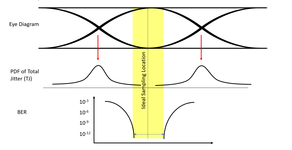
Together, these (and other effects such as reflections) reduce eye opening and increase the Bit error rate (BER) at your sampling edge.
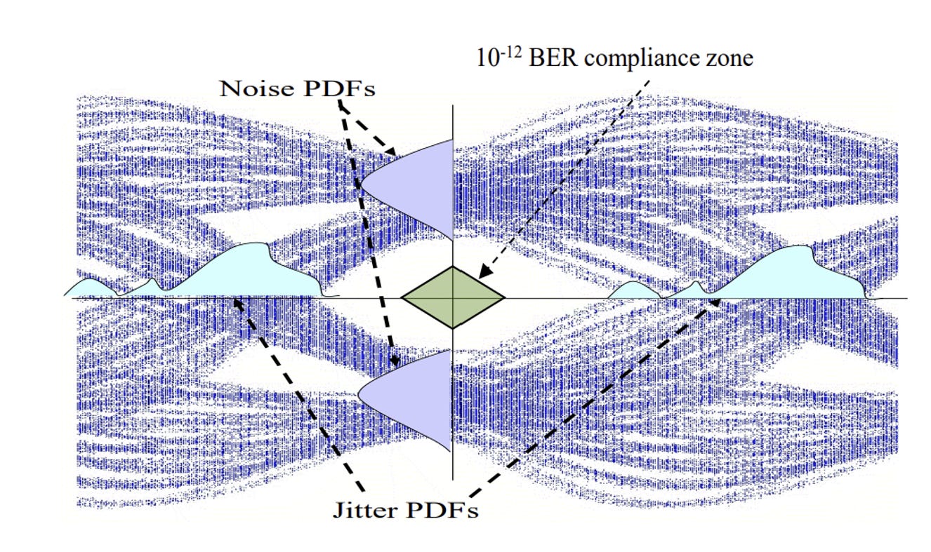
Bit error rate is not easy to measure directly because of the amount of time it takes to observe enough samples (sometimes trillions) to get a statically significant measurement of BER. It is usually easy to measure a BER of 10^-6 which is 1 error in 1 million bits with a BERT (Bit error rate tester), but some systems require BERs of 10^-12 which is one error in one-trillion bits!
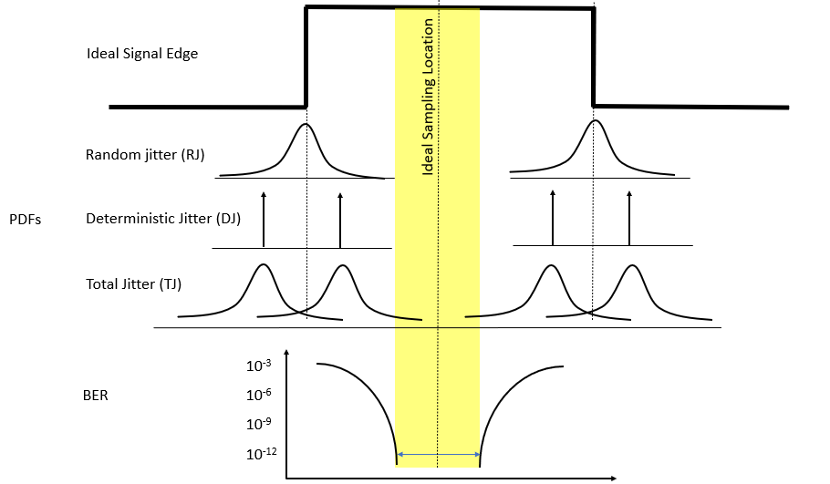
Often, lower BERs are often extrapolated from higher BER curves. The Dual-Dirac model is a widely accepted “worst case model” used to extrapolate this. To show how BER is driven from jitter, consider the two major classes of jitter:
RJ spreads the signal edge according to a Gaussian distribution
DJ shifts the signal edge with two “bounds”. In this model, the worst cases are represented as two worst case impulse ”spikes” at either bound.
(Note that this is not the actual PDF of the DJ as it varies in uniformity within the bounds. However, this works fine because we only care about the “tails” of the RJ curve convolved at the bounds)
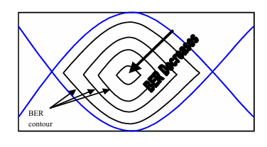
These two sources combine in a “convolution” format, so the gaussians of the RJ map onto the bounds of the DJ to obtain the Total Jitter (TJ). The BER is then estimated from the tails of the total-jitter distribution: as the distribution spreads further into the sampling margin, the probability of error increases.
You can then use this to map contours of constant BER in the center of the eye that decrease the more the signal is sampled at the center of the eye:
Major System Trends: PAM-4 and DSP-based Architectures
PAM-4: 4 level pulse amplitude modulation
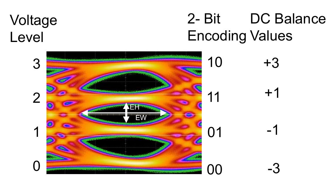
PAM-4 uses four levels of modulation instead of two. This allows you to transmit two bits per symbol while halving the required symbol rate for a given bit rate.
However, added signal levels make PAM-4 more sensitive to noise, nonlinearity, ISI, and timing jitter. It also requires DACs to generate the four analog levels. There are also more transition combinations to account for.
DSP-Based Transceivers
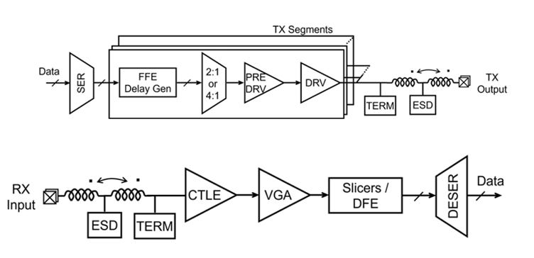
When data speeds were slower, most of the processing came from analog circuits that were sufficient to perform the signal conditioning needed to achieve good BERs. Figure 9 shows a typical short-reach, analog-based transceiver with common building blocks.
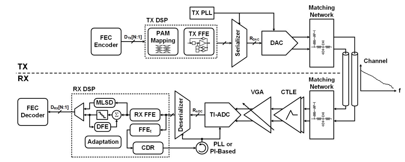
As speed and throughput increased, most architectures added a lot of DSP along with the analog blocks. Digital allows a lot more programmability to handle data processing with FIR/IIR filters. However, digital also adds a large amount of peripheral complexity to handle the speed it needs, including:
The ADC/DACs needed to convert between the analog and digital domains
The clocking architecture to clock the circuits
Error Reduction Techniques
After the paywall, I’ll cover key error reduction techniques, including equalization, FEC, CTLE, and DFE.
If you want to continue expanding your knowledge related to signal integrity, including why modern SerDes is so complex, check out my other posts:

