
Design Automation Conference 2026 - Why AI Will Not Replace Chip Designers Anytime Soon
VLSI fundamentals, vibe coding RTL, why chip design takes so long, and key bottlenecks that limit AI use in chip design to quality-of-life enhancements

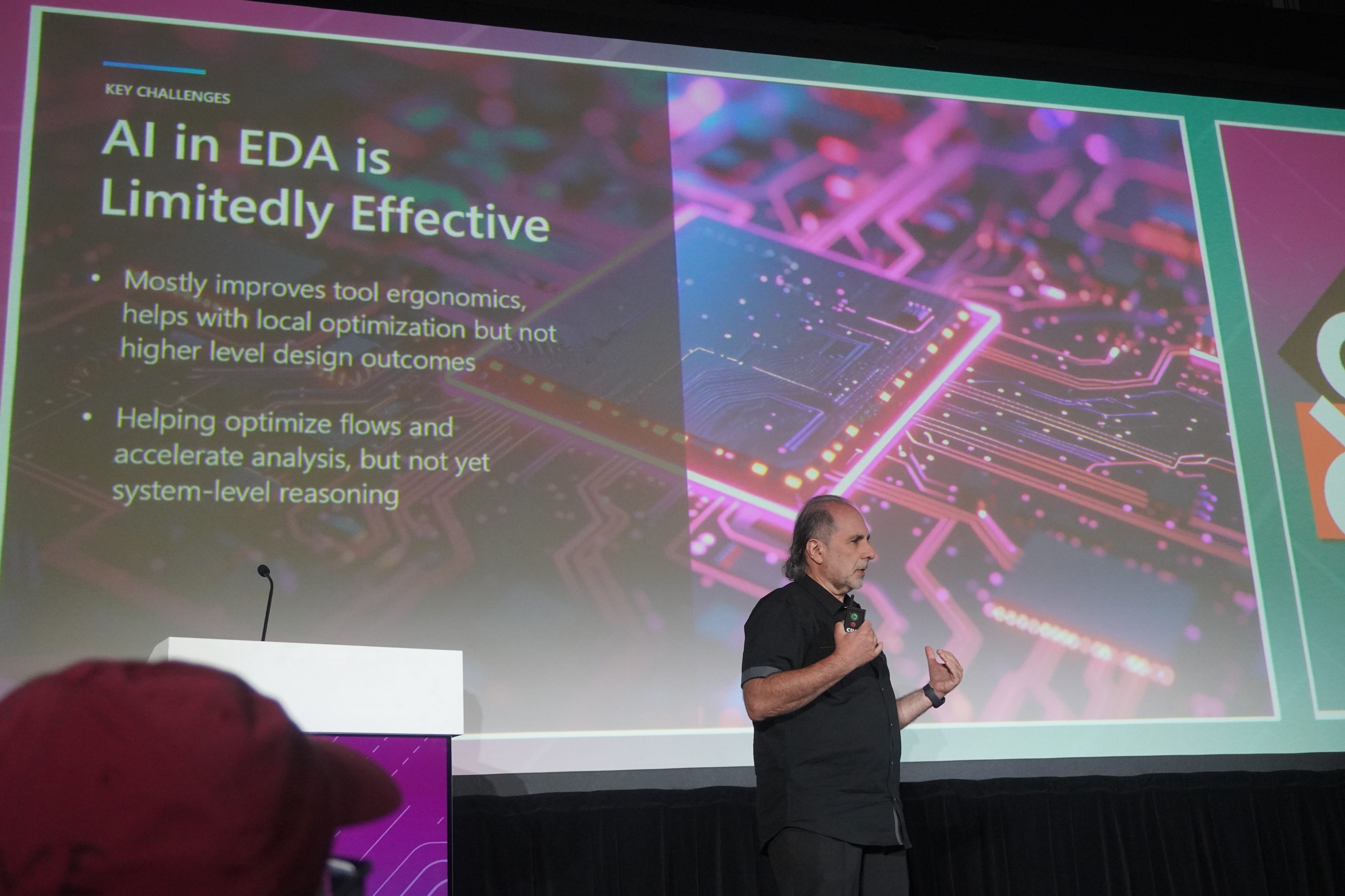
AI will not replace chip designers anytime soon. In fact, AI has made chip design even harder in many ways. This post will illustrate why from first principles by covering the following topics:
High Level Overview of VLSI Design Process
Vibe Coding RTL – Systolic Array example
Benefits and Risks
Why Chip Design Takes So Long: Cost of Error due to Fab Bottlenecks
Key Bottlenecks that Limit AI use in Chip Design to Quality-of-Life Enhancements
🔒Functional Verification
🔒Physical Co-design: Modularity and Thermal/PDN/SI/Packaging Constraints
🔒AI-Driven Design Space Exploration
🔒The Hidden “Memory Wall” - Compute Resource Bottlenecks
I went to the floor of the Design Automation Conference on July 26-29 in Long Beach, CA. This is conference #5 of a broader conference tour this year (ISSCC, DesignCon, APEC, and ECTC) where I’ve worked my way up in abstraction levels to better understand the complete AI datacenter stack and educate you on it.
I’ve noticed a lot of prominent writers who don’t know much about chip design speculate about how Agentic AI will impact it. Most people assume that AI will have the same disruptive impact in the SW and chip industries since software and RTL code can easily be generated with LLMs, creating a lot of FUD.
I’ll highlight the benefits of AI with a vibe coding tutorial of RTL and how chip designers can benefit. Then I’ll show the critical flow differences in chip design that need to be scrutinized and cause veteran engineers to not completely trust AI.
Please note that I have more experience in analog / mixed signal design, not digital design. I have interfaced with digital / verification people and written my share of VerilogAMS to have a working understanding of the VLSI design flow. I reference the book “VLSI Physical Design: From Graph Partitioning to Timing Closure” for more detailed flow information.
As always, if you’re an expert in this area and notice a mistake, please reach out to me so I can have it promptly corrected.
High Level Overview of VLSI Design Flow
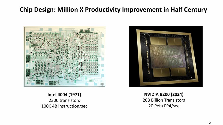
Chips have become much more complex over the years due to a well known phenomenon of Moore’s law. Moore’s law enables more transistors to be placed and doubling compute density about every two years. Very Large Scale Integration (VLSI) is the umbrella term used to refer to the tight integration density of the various classes of chips (SoC, GPU, ASIC, FPGA).
Automation is necessary for chip design because of the sheer design complexity and errors in chip designs are much harder and costly to fix that board-level errors. As a result, the entire EDA industry revolves around robust automation tools to perform a lot of complicated steps automatically. Only low-level JP and customized analog blocks tend to be hand drawn and instantiated by the tool at higher lever assemblies.
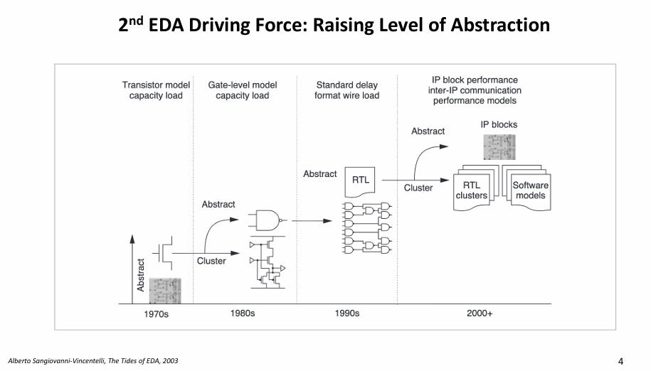
At a DesignCon keynote “Agentic AI for Chip Design”, Mark Ren, founder and CEO of AGENTRYS, notes how EDA tools flow raised the abstraction level that humans operate at. AI enables an even higher level of abstraction by allowing engineers to specify design intent in plain language rather than a specific programming language.
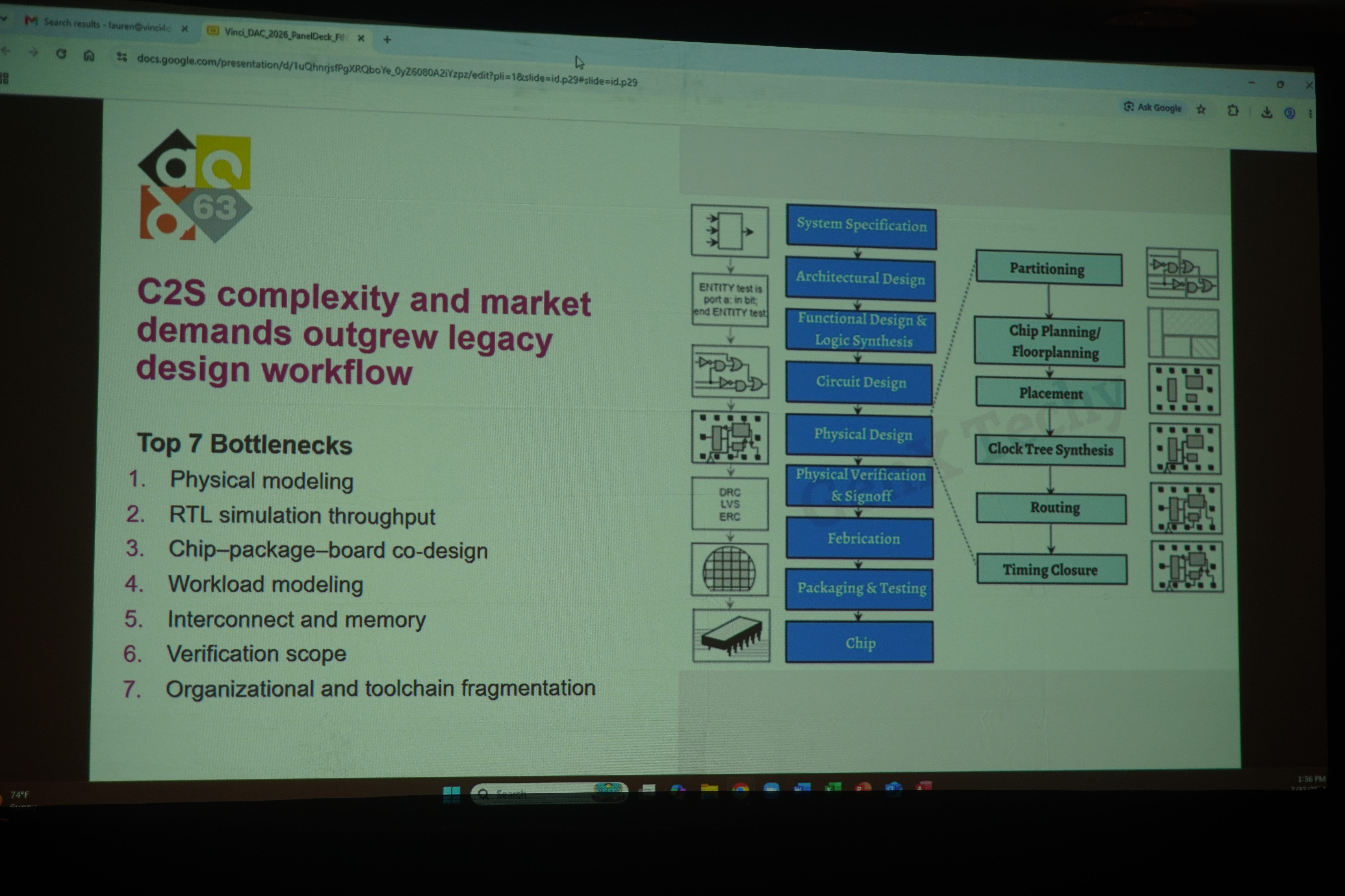
The goal of the VLSI design process is to produce a fabricable, error free mask that implements the desired system specification within the constraints of the fabrication Process Development Kit (PDK). The VLSI design process evolved over time to incorporate the following major steps:
System Specification. The overall high level goals of the system are defined collectively amongst chip architects, product marketers, and ASIC engineers
Architectural Design. An architecture must be defined to achieve the high level goals of the system. These include:
Analog/Mixed-Signal Blocks - ADCs/DACs, regulators
Digital Blocks - DSPs, and types of computational blocks
Interfaces - I2C, UCIe, PCIe
Hard / Soft IP
Packaging
Clocking Architecture
Process Node
Functional Design and Logic Design - Logic design is performed at the RTL level using a HDL such as Verilog or VHDL.
Custom Circuit Design - A handful of critical blocks such as ESD protection, I/O, analog circuits, and RAM blocks have to be hand-designed.
Companies can develop these IP in house with library / IP teams across major projects or license IP from specific vendors.
In some cases of one-time jobs, such as customized analog blocks, companies can utilize contract labor to complete the work if there is not a steady workload for a W2 employee.
Physical Design - The RTL is synthesized and billions of design components get instantiated with their geometric representations using highly sophisticated Place-and-Route Tools. Physical design is highly iterative and includes the following steps:
Partitioning
Floorplanning
Placement
Clock tree Synthesis
Routing
Timing / Power Closure
Physical Verification and Signoff. The layout needs to be checked against different design rules defined by the fab (DRC, LVS)
The design needs to be officially “signed off” by specific tools to keep a paper trail should errors arise down the line. These tools often have valuable information in the logfiles that can pinpoint sources of errors. Design waivers can be made to in special circumstances to overcome tool constraints and are agreed upon in design reviews, but are generally avoided at all costs.
Fabrication - The final layout is streamed out as a GDSII Stream format and is sent to a fab.
Packaging and Testing - The chips are packaged using appropriate package types such as DIPs, PGA, BPA, flip chip, or WLCSP.
The design flow is iterative, with engineers making design choices at each step based on simulation feedback before handing off the work to the next step.
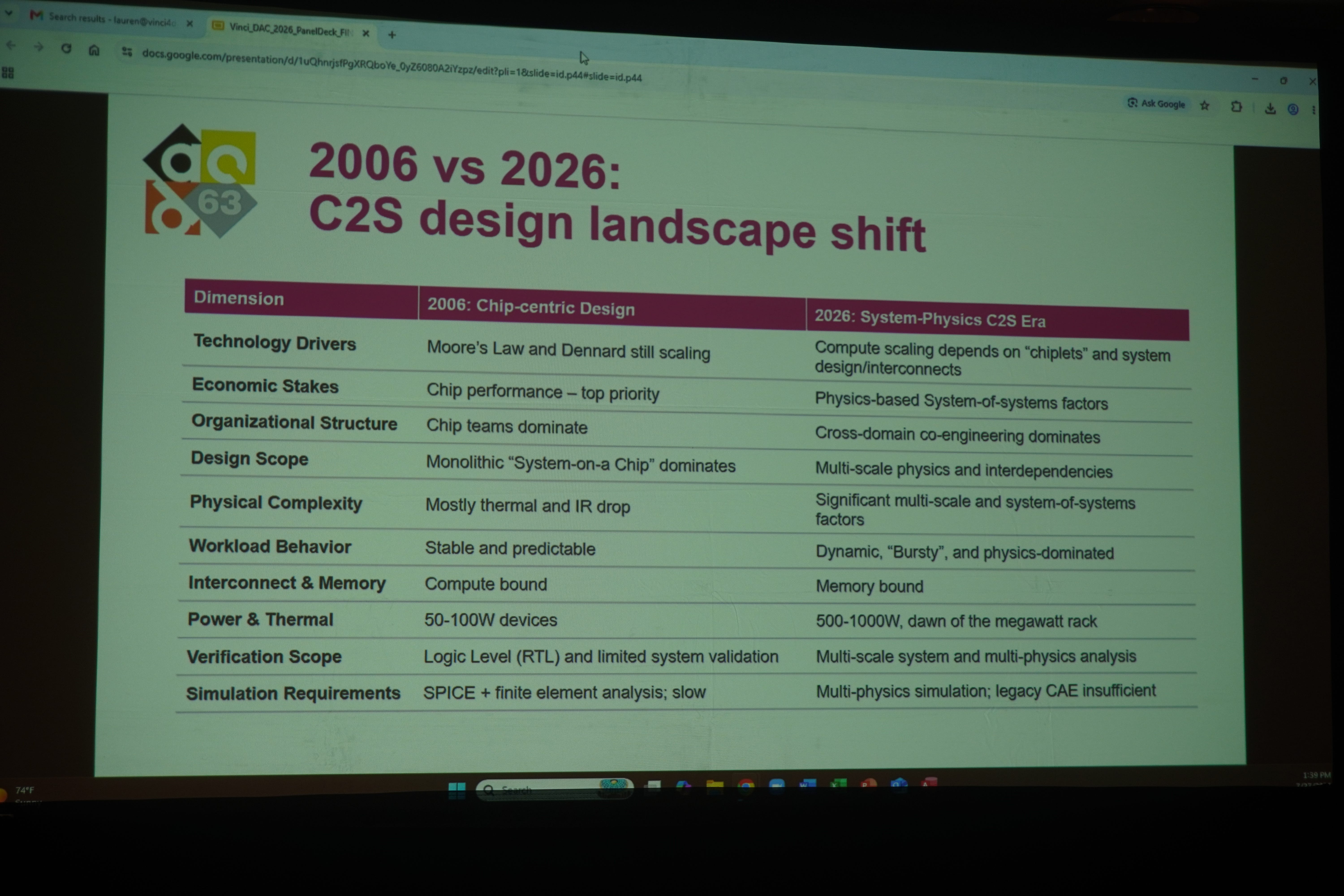
Chip design has historically been siloed with well-defined specialties and tool flows developed within each specialty to maintain consistent flows along process node improvements. This approach has worked to scale chip performance for a number of years, but the slowing down of Moore’s law and multiphysics constraints had led to a paradigm shift toward cross-domain engineering. This approach requires a shift in engineering mindset that is not always easy to transition to due to entrenched organizational incentives. This substack aims to facilitate that mindset shift by making cross-domain information easier to access.
Vibe Coding RTL – Systolic Array example
Before I talk about the challenges of AI for chip design, I’ll highlight a positive example of how AI can benefit chip designers: code generation of RTL.
At the beginning of DAC, Steven Truitt, Nan Wu, and Liu Liu gave a very good tutorial “From Vibe Coding to Silicon: Engineering Agentic Systems for Hardware Design” using Microsoft Discovery. Their GitHub is public at the following link that you can check out:
https://github.com/stevetru1/DAC2026_Vibes
https://github.com/ORCA-lab/DAC26_VibeCoding_Runs
What is Vibe Engineering
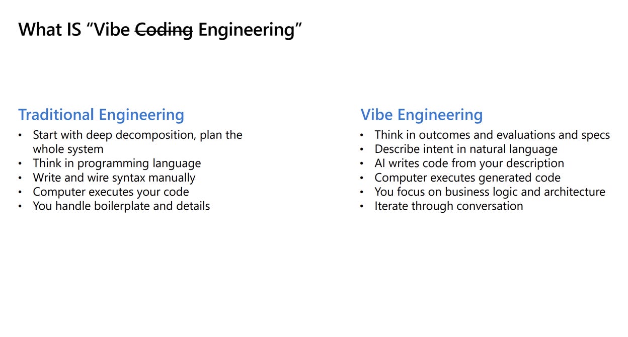
Vibe engineering is the hottest trend in SW engineering that enables non-SW engineers to code SW and offers productivity enhancements for junior engineer-level tasks. Vibe engineering can also apply to the SW portions of chip design, including RTL coding.
Vibe engineering involves thinking an abstraction level higher than traditional engineering. You rigorously describe your intent in terms of the desired outcome, rather than the programming language, for your agent to perform. The design is iterated on through conversation and feedback loops based on what the agent produces.
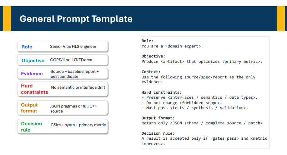
Here is an example prompt template where the desired outcomes are rigorously specified for the agent.
One important consideration in vibe engineering is defining the definition of done. Task organization up front is extremely important to properly decompose, organize tasks, and build the harness flow for the agent to execute in. The test and evaluation suite is also very important to evaluate agent performance properly.
Vibe engineering places more emphasis on judgement in execution rather than execution expertise. The challenge is figuring out the right thing to build, instead of building faster. As a result, the human layer carries more weight.
Example: Systolic Array
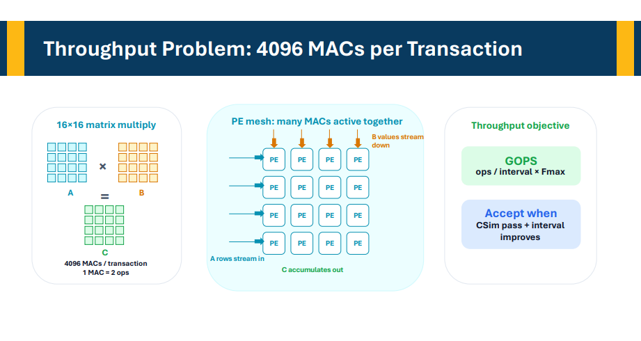
One key block in AI accelerated ML applications is the systolic array. Systolic arrays are often used for AI acceleration and are typically co-designed to the specific data needs. I’ve written on Systolic arrays previously in my other posts.


A description a vibe coder might give an agent can look something like this:
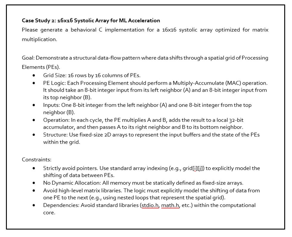
Now I’ll admit: I hate writing RTL code, even though I have taken a Verilog and VHDL class, so I find this vibe engineering approach such a breath of fresh air.
More detailed information can be found in the slide decks and tutorials; I’ll leave it up to you to check those out.
Why Chip Design Takes So Long: Cost of Error due to Fab Bottlenecks
Chip Design is one of the most brutally unforgiving industries because chip design is very expensive, time consuming, and carries a high cost of error.
In board-level design, any design errors can be easily fixed after fabrication because the device is more interpretable and technicians can workaround issues such as adding jumpers and lifting off pins. As a result, there is less scrutiny during board design because components with datasheets can be hooked up with passives in between and simulated in SPICE at a high level.
Chip design has way more components than boards and does not offer that deep of a debug capability to probe deep inside the circuit. Test modes and circuits for DFT must be inserted such as scan-chains and test mode registers. It takes 3 - 4 months for a chip to be fabricated because each individual fabrication step can take days due to manufacturing queue times and tool bottlenecks.
First Pass Silicon Success
Generally speaking, there is a low pass rate of first pass success, around 14% nowadays. This might come at a surprise for outsiders, but not unexpected for engineers as schedules typically account for this. For most practical purposes, the first silicon revision is used to identify bugs that weren't caught early on, and the second revision is used to fix them. Two revisions are generally considered standard, with some CEOs like Intel’s Lip-Bu Tan threatening to fire engineers who exceed this.
There are a few ways to minimize time delays and errors:
Pre-Silicon Emulation. The design is loaded on an FPGA or hardware array to make sure the design is bug-free. Emulation is much faster than computation-heavy simulation and typically run at lower clock speeds to test specific test cases and interactions within blocks.
Pre-Silicon Prototyping. Not only does the chip has to work as designed, it also has to work as intended in the broader system context. Prototyping serves an important function to ensure you build the system you intended, not the bug free one you built.
IP Reuse. Almost all new chip designs have a starting point with known good IP blocks. Low risk IP can be incorporated in a new design, and new IP to implement the performance requirements needs to be modified or created out of scratch. The overall design risk is assessed based on the risk of existing and new IP blocks themselves.
Wafer Staging. During fabrication, several wafers are “staged” where only the time-consuming FEOL layers are formed. In case of bugs identified early that can be fixed in metal-only, this shortens the fab time to get wafers back without having to go through the entire PnR flow all over again.
Companies generally name revisions A0, A1, B0, where A0 is the first revision, A1 represents a metal change, and B0 represents a whole new silicon revision with a new mask set.
The fabrication cost and time is largely dictated by the # of masks since each tool loads a specific mask.
First pass silicon success is really only feasible when either the chip is simple enough, there is enough existing IP that is leveraged, or there are heavy emulation/prototyping efforts. Some companies who want to specifically integrate specific circuits want to see a test chip done first, key data taken, and risk evaluated before committing the chip to be integrated in their product in the next revision. General market products can be a bit more lax.
Scar Tissue
The long fab time and cost of error leads to a less discussed phenomenon in the chip industry: scar tissue, which is a form of lessons learned painfully through delays and expenses.
Scar tissue is one big reason why experienced silicon veterans often push back against claims that AI will “autonomously design chips” because it doesn’t carry accountability. This lack of accountability for AI tools means that it won’t replace human designers anytime soon.
Key Bottlenecks That Limit AI use in Chip Design
I’ll discuss four key bottlenecks that several panelists at DAC raised and promising solutions within them.
Functional Verification
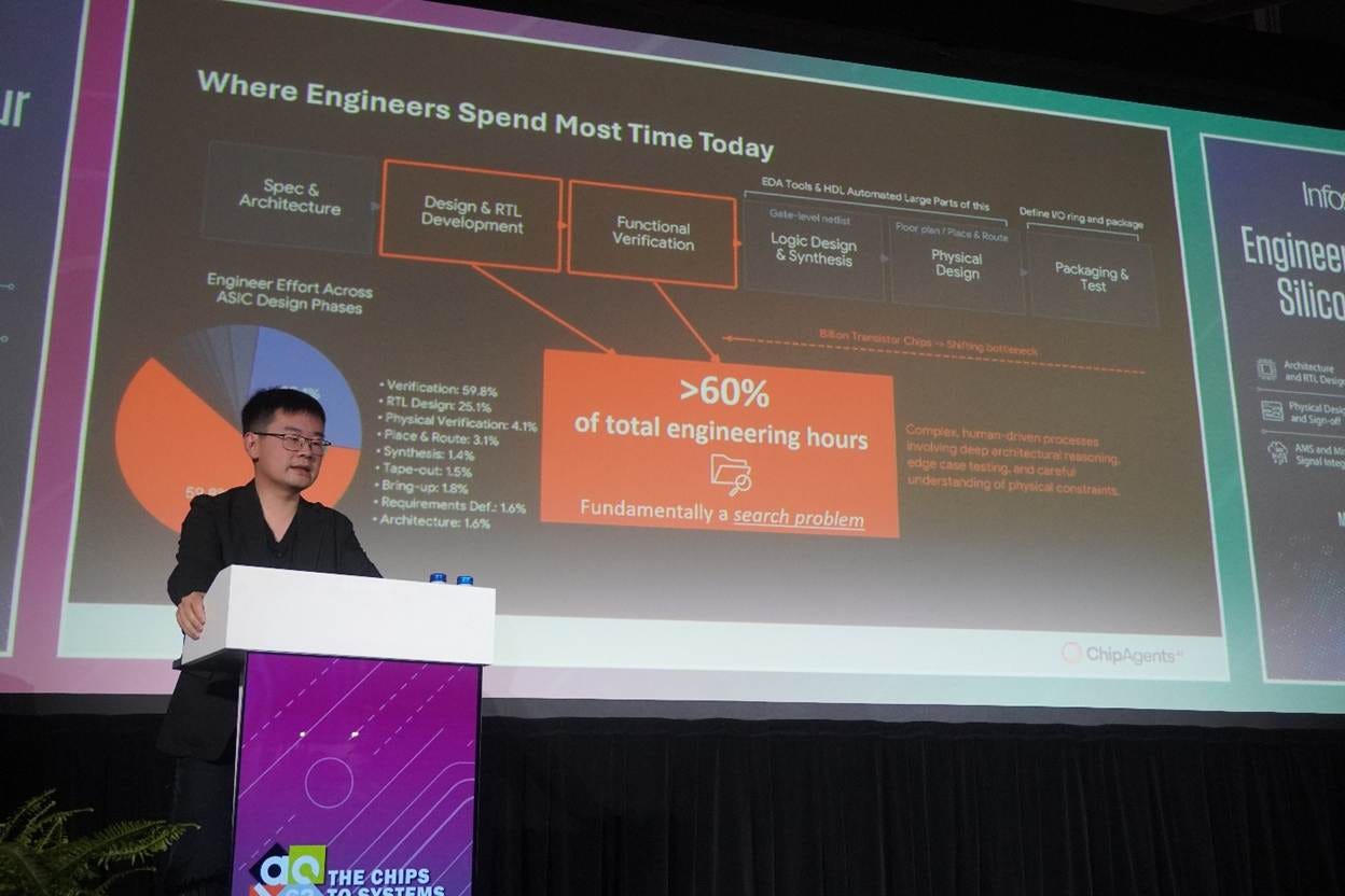
Most people outside of the semiconductor industry don’t know that verification, not design, has historically been the most labor and time intensive task. Let me give a bit of context to what verification should be, and how its implemented in practice.