
A Deep Dive into SRAM: The Staging Ground of LLM Inference
Fundamentals of SRAM and how SRAM constraints affect array size scaling and LLM inference performance

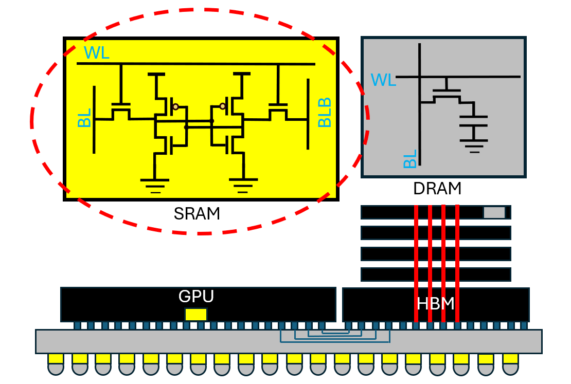
In this post I will cover the following topics on SRAM:
6T SRAM Fundamentals
Cell Structure
Strong / Weak Switches
Principle of Operation: Read
Principle of Operation: Write
Key Tradeoff: Read Stability vs Write Margin
Cell Layout
Challenges with Scaling Large SRAM arrays
🔒SNR
🔒Interconnect RC
🔒Common Optimization/Assist Techniques
🔒Optimizing Transistor Sizes of Embedded SRAM Bit Cells
🔒Opportunities and challenges designing SRAM in FinFET and GAA process technologies
SRAM is a very important memory because it is the fastest memory in the memory hierarchy that can be integrated directly onto the same piece of silicon as logic transistors. However, SRAM is limited by capacity and cost, which largely limits it to smaller local on-chip cache memory.
SRAM is perhaps the second most important memory in LLM applications (after HBM) because it is the staging ground where values from KV Cache are written to from HBM. The size of the SRAM directly influences the maximum amount of local data available to local compute. Larger SRAM sizes minimize memory transactions with the HBM and maximize bandwidth density with the compute.
Thus, I believe a high-level understanding of the fundamentals and constraints of embedded SRAM is essential for AI researchers and HW engineers alike who all wish for bigger SRAM bank sizes.
The following post references content from the ISSCC 2026 tutorial I personally sat in, “Memory and Logic Circuit Design in Technologies Beyond FinFET” by Zheng Guo of Intel. This tutorial comprehensively covers the real-world nonidealities and scaling challenges of SRAM in FinFET and GAA process technologies. Though SRAM with GAA has not shown meaningful memory density increase, it’s still worth considering the challenges with GAA to better inform future SRAM designs.
I’ll cover the most important memory, HBM, more comprehensively after Hot Chips since there are several excellent tutorials lined up during the conference. I already covered a few signal integrity scaling challenges of the “wide and slow” approach in this post from ECTC:

6T SRAM Fundamentals
SRAM is a fundamental memory commonly taught in undergrad VLSI classes. Students are often given an assignment to design and optimize an SRAM cell as it illustrates a few fundamentals of how transistors are physically implemented and integrated, as well as fab design rules. I remember being assigned an SRAM project where the project grade was based on how tightly you optimized the PPA of your SRAM cell and array size compared to others in the class. You can imagine how motivated the class was to squeeze out as much performance out as possible and not leave any performance on the table. That reflects how tightly optimized SRAM cells need to be across PPA.
Cell Structure
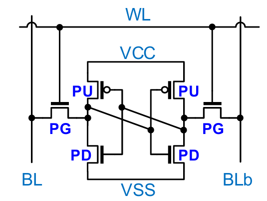
At its core, SRAM stores data as a “state” across a cross-coupled inverter where the output of each inverter is connected to the input to the other. These inverters are implemented with the following transistors:
Pull-Up - PMOS transistors connected between VCC and Signal.
Pull-Down - NMOS transistors connected between GND/VSS and signal
Each node of the cross coupled inverter is connected to the bit lines through pass gates, which are NMOS switches that control the current flowing through it from a wordline voltage.
In traditional digital logic gates, the PMOS W/L is typically sized larger since hole mobility in PMOS tends to be lower than electron mobility in NMOS. However, in SRAM, the pulldown NMOS is actually sized much larger. We’ll see why this is.
Strong and Weak switches
The terms “strong” and “weak” switches often get conflated with “fast” and “slow”. These terms are also interpreted differently amongst analog, digital, and memory engineers. Even I get confused sometimes. Let me first make the distinction between the two set of terms.
When a transistor operates in saturation mode, the current is given by the following equation:
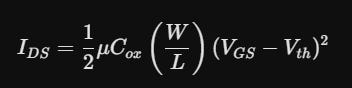
This mode is commonly used for “controlling” the amount of current, much like you would turn your shower knob to control the flow of water. In SRAM’s case, the pass gate operates in saturation to allow read current to flow through.
During circuit design, designers have control over the length and width of the transistors. Wider widths and shorter lengths mean more current passes through, so switches with a higher W/L ratio are said to be “strong”. I dive more into analog sizing conventions here:

There are several other parameters in the above equation the designer does not have control of, but must account for variations in. These include the electron / hole mobility un/up (NMOS/PMOS), the gate oxide capacitance Cox, and the threshold voltage Vth.
In the analog world, the device parameters of these models are lumped and abstracted into 3-σ corner models - SS, SF, FS, and FF - that correspond to NMOS/PMOS combinations. 3-σ represents the systematic range of on-wafer process variation; a die on the center of the wafer can have systematic shift in one parameter compared to dies on the edges of the wafer. You don’t want to scrap large parts of the wafer because of this systematic shift.
These corner models tweak various internal FET parameters that affect circuit performance, including the switching speed, drive current, and offset. These model parameters are characterized and correlated by the fab in their process control measurement (PCM) circuits. Designers cannot touch or even look inside of these models.
For each block designers build, the performance requirements must be verified with sufficient Monte Carlo simulations across these corners to ensure robustness against variability. This, in my opinion, is “grunt work” that AI can potentially automate.
When masks are fabricated, fabs will intentionally skew a few wafers in a lot into “splits” of SS, SF, FS, and FF wafers. This way, PTE and Post-Si Validation can characterize and screen these to properly quantify yield. Additionally, the wafer location where the chips originated from are well-tracked.
Yield depends on the worst case device among the # of devices being fabricated. SRAM and digital circuits consisting of millions or billions of repeated transistors have to yield out to 6-7 σ, whereas analog circuits consisting of 100’s or 1000’s of manually tuned transistors have to yield out to 3-4 σ.
Principle of Operation: Read
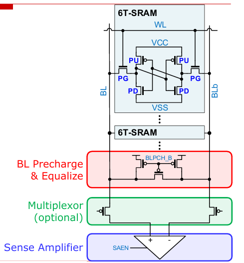
The read operation works in the following way:
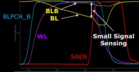
First, the bit lines are precharged and equalized with a signal BLPCH_B that charges both BL and BLb to VDD through PMOS switches.
Then, the wordline is asserted to turn the PG on and cause a differential signal across both bitlines
One BL voltage is pulled down by discharging the BL capacitance with a read current
During this read process, the PG and PD form a resistive voltage divider that raises the internal SRAM voltage slightly, but not high enough to flip the state.
A MUX switch is optionally asserted if multiple lines share the same sense amplifier
The sense amplifier is triggered after a period of time and amplifies this differential signal
The BL is pulled down enough for the sense amp to properly distinguish between a 0 and 1.
There are two nonidealities when the line is discharged too slowly and too quickly:
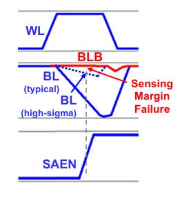
Read errors and SNR degradation can occur when the line is discharged too slowly due to the sensed differential signal not meeting a minimum threshold. This is affected by all circuit parameters, including read current, BL leakage current, bitline capacitance, and the offset voltage in the sense amp.
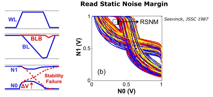
Stability failures can occur when the internal node voltage rises too much. Depending on the mismatch between transistors, the internal voltage nodes can end up flipping the memory state when it’s not supposed to due to charge injection. This is often quantified as read static noise margin.
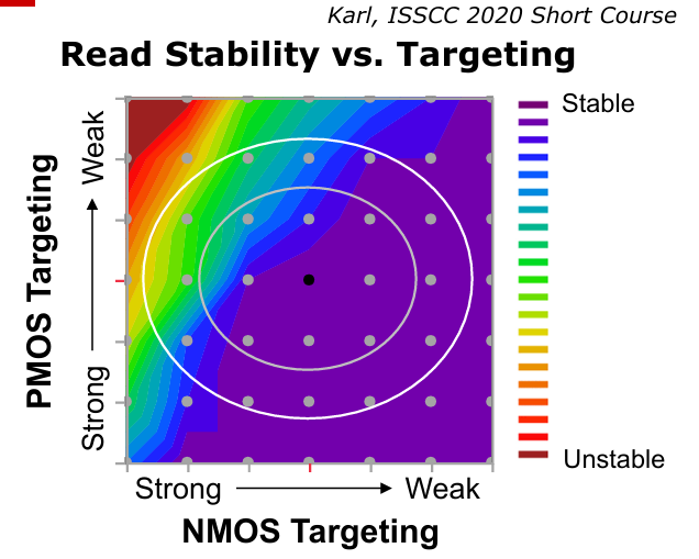
Here we see a broad range of relative NMOS-PMOS size targeting and how they impact read stability.
Principle of Operation: Write
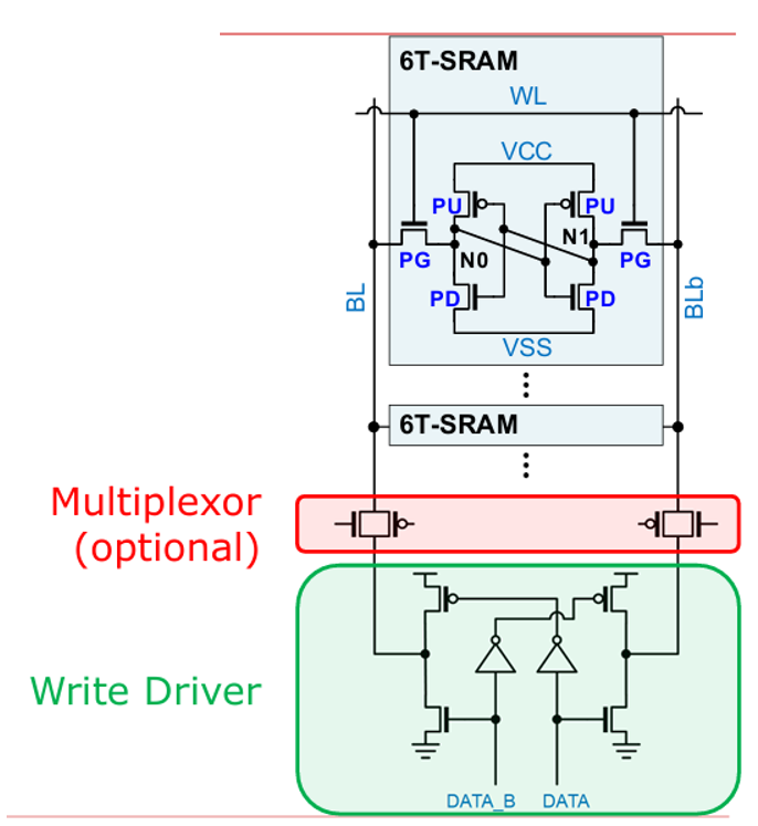
The write operation works in the following way:
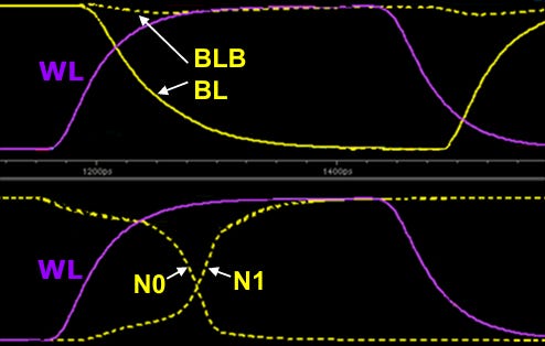
The input, DATA/DATA_B pull one line down from VDD to GND
WL is asserted to update the internal nodes N0/N1
In order to successfully write a 0 or 1, the series combination of the write driver PD and the PG must be significantly stronger (i.e. lower resistance) than the cell's internal PU transistor. This is determined by the ratio between the PG and PU sizes which is given by:
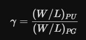
If this ratio is too high, the gate cannot flip, resulting in a write margin failure.
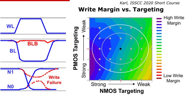
Key Tradeoff: Read Stability vs Write Margin
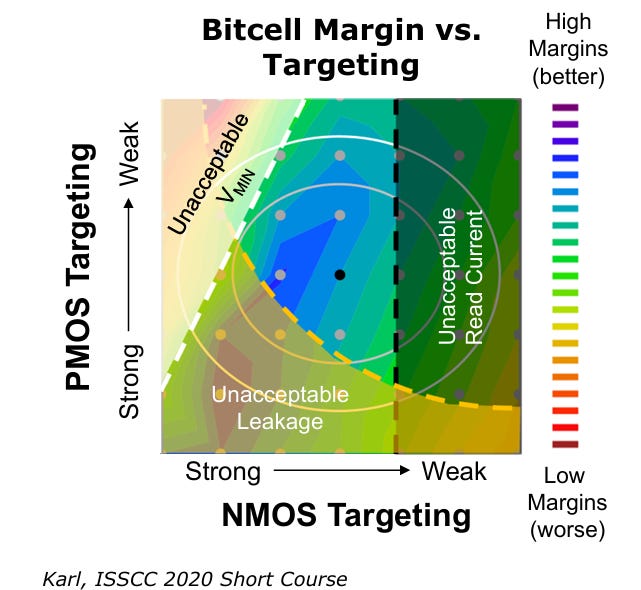
The conflicting requirements of read and write margins result in an operating space that the SRAM can acceptably operate in over relative device sizing.
Here we notice three regions that cause low margins:
When the NMOS is weak, this causes an unacceptable read current
When both PMOS and NMOS are strong, this causes unacceptable leakage
When the PMOS is weak, this causes unacceptable Vmin
Depending on the size of the banks, high-σ methods are needed to characterize process variation to determine the best global optimum to ensure the SRAM stays within this region, with 6-7 σ being the gold standard. ML-aided tools like Solido aid to search this space since quantifying 6-7 σ with brute force simulation eats up tons of compute time and licenses.
These SRAM can also be modified for compute-in-memory applications. I discuss that in more detail in my post:

Cell Layout
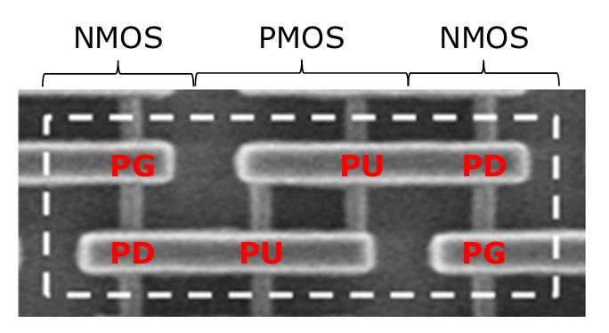
Here is a common compact implementation of SRAM. The horizontal lines (poly) are the gates that control the flow of current through the vertical channels with VDD and ground located above and below the cells.
Challenges with Scaling Large SRAM arrays
There are several challenges with scaling SRAM arrays and common ways to handle nonidealities, which will be discussed more after the paywall.
I wrote a high level article that puts SRAM in its proper perspective, using Eyeriss as a case study:

In addition, Vikram Sekar’s and Subbu’s SRAM post cover a more high-level look into SRAM and DRAM. This is a good companion piece to round out your knowledge.
