
A Comprehensive Overview of the AI Accelerator Landscape: From Digital to Analog Compute-in-Memory Architectures
A survey of major AI accelerator categories, and a deep dive into the scaling challenges with Analog Compute-in-memory

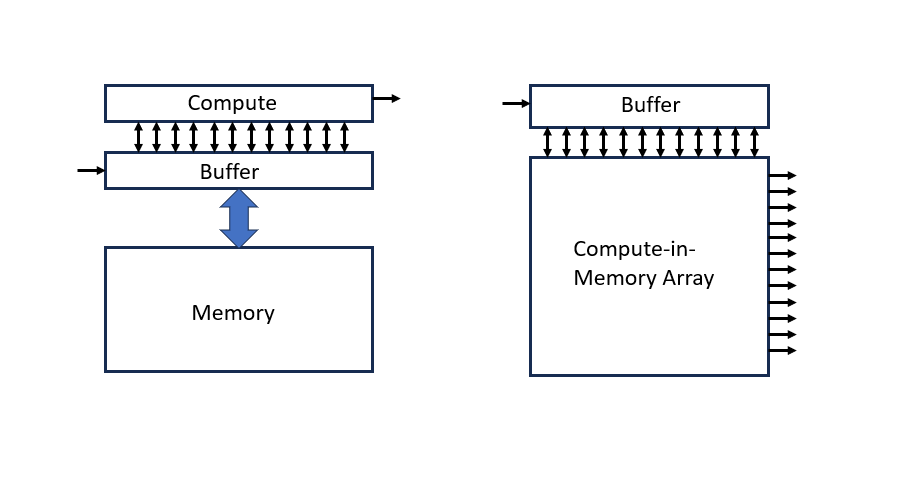
Compute-in-memory has emerged as a promising technology to overcome the Von-Neumann bottlenecks of conventional digital computing. Many venture-backed startups have entered this space with promising solutions to enhance compute efficiency.
In this post I’ll cover a broad overview of the AI accelerator landscape and do a deep dive into the challenges with scaling Analog Compute-in-memory. The outline of this post is as follows:
A Survey of the AI Accelerator landscape
Application Spaces - from VLP to Data Center Systems
Scaling Trends - Co-Design and Specialized Architecture
Hardware Classifications of Compute in/near memory AI Accelerators
Parallel Threads (NVIDIA GPU)
Tensor Array (Google TPU, Groq)
Manycore Accelerators (Cerebras, Tenstorrent)
Digital Compute-in-Memory
🔒The Building Blocks of Analog Compute-in-Memory
🔒SRAM Arrays
🔒Input Encoding
🔒Charge / Current Domain Devices
🔒Scaling Challenges with Analog CiM
🔒Array Nonidealities that degrade SNR
🔒Area Inefficiency
🔒Modality Conversion Overhead
🔒Example CiM startup: Encharge AI
🔒BONUS: The Challenges of Optical Compute for AI
Back in February 2026 at ISSCC in San Francisco, CA, I personally sat in the tutorial “Fundamentals of Compute-in-Memory: From Circuits to Systems” by Prof. Jaydeep P. Kulkarni at the beginning and an all-day forum “Analog for AI and AI for Analog” at the end. Several heavyweights in the analog community such as Prof. Naveen Verma and EDA community such as Prof. David Pan were present to discuss trends in Analog CiM and Automation for AMS/RFIC Signal Design, the latter of which I will eventually cover after DAC.
Personally, analog compute-in-memory is one of my favorite topics because it almost resembled the way the brain processes data. Analog CiM is perhaps the most interdisciplinary topics among semiconductor specialties because it combines knowledge from digital, mixed signal, logic fabrication, and memory domains. I think the circuits are inherently power efficient for repetitive computations.
However, the CiM space is filled with a lot of dense academic research and marketing claims of VC-backed companies. During those ISSCC sessions and while researching CiM papers, I initially found CiM difficult to digest because there aren’t universally agreed on standards to classify related architectures. The terminology is also inconsistent; some authors use compute-in memory, others use processing-in-memory, and other add subcategories of their own. Moreover, most papers tend to jump right into the block diagrams of specific applications known among academics in that space. I’m sure many of you also feel the same way trying to understand the space.
In my opinion, CiM is a space where broad system benefits can be lost in the vast chasm between marketing claims and actual technical challenges. I believe that researchers are candid about the real engineering challenges. However, claims of performance benefits tend to narrowly focus on the energy savings of ONE part of the whole computational energy budget. These claims tend to get picked up and hyped up by non-technical people without their proper nuances, which, for some companies, is a marketing strategy all in itself.
Having sat in those rooms and felt the confusion myself, I aim to bring clarity to the space. Here are some of my previous posts I’ve written that lay a foundation for this material from both the software and hardware side:


A Survey of the AI Accelerator Landscape
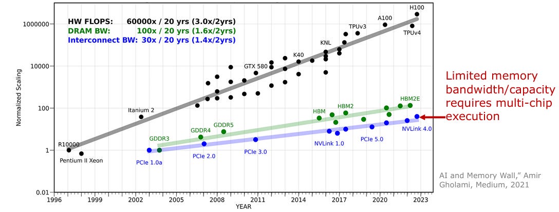
GenAI and Agentic AI models have exploded in the past few years with a combination of gigantic training sets and powerful models to handle a variety of AI applications. This creates a huge demand for tokens for Agentic AI that is primarily satisfied by high power, general-purpose data center GPUs in data centers.
The underlying hardware is becoming more powerful to satisfy this demand. However, the logic is scaling much faster than the memory and interconnect by approximately ~2x. This means that the compute bottleneck is not in the compute itself, but the data movement. As models become more powerful, memory transfer operations are consuming more and more energy and latency.
As a result in the explosion of compute power, co-packaged optics and vertical power delivery are emerging and widely discussed trends to satisfy these demands. I have written extensively on these topics on my website.
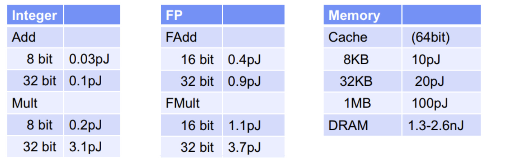
One of the main arguments for CiM is to minimize the power overhead in compute-memory transfers. Here is a prominent slide given in 2014 with ballpark energy consumption of various computational operations and memory accesses. Notice the order of magnitude difference between the energy used in cache and DRAM accesses, and the higher energy consumption for higher precision operations. This chart has driven a trend toward lower precision computations in the digital domain and memory efficient architectures.
Application Space - from VLP to Data Center Systems
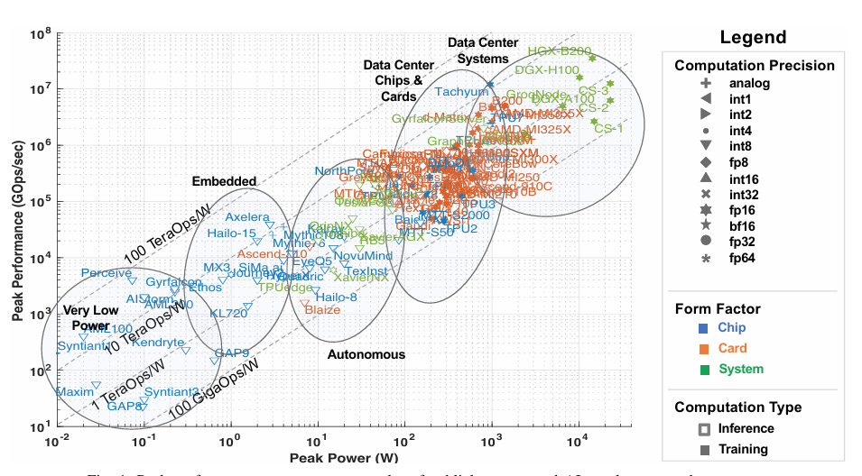
AI accelerators are not just limited to centralized data center GPUs, but also embedded applications with many different form factors and use cases.
Here we notice a range of publicly announced accelerators that range in compute efficiency from 0.1 - 100 TOPs/W. Notice how there is a cluster primarily centered around 1 TeraOps / W for general purpose GPUs data centers. Also notice how at lower power, accelerators specialized for embedded applications tend to have higher TOPs/W because they are tailored for the specific power / performance / form factor requirements of the system they are in. In those cases, it doesn’t make sense to stream data to a centralized data center to run inference on.
General purpose GPUs are built to support both training and inference across a broad range of AI models targeted for different applications, depending on the tasks you throw at it. Two common applications include:
CNNs: Uses deep neural networks to extract lower level features and are used for image / speech classification
LLMs: Uses attention layers to calculate relations between words using Query, Key, and Value vectors and require large KV cache storage for long sequences
Scaling Trends - Co-design and Specialized Architecture
Massive scale-up of AI clusters are driving a huge need for compute efficiency. Large networks of parallel general-purpose GPUs move a lot of data around, consuming vast amounts of power and generating a lot of heat in the process.
To address this need for more compute efficiency, the industry is shifting from general purpose to hardware-software Co-Design (or co-optimization) of both DNN Models and Hardware.
This involves customizing the HW to be as efficient at computing its specific task. Some optimization examples include:
Memory: Higher bandwidth and more tightly integrated memory
On the SW Side:
More aggressive quantization / lower precision architectures
Sparse weights
HW architecture: Stationary architectures that “fix” one value in an array and stream in the other (weight, output, and input)
In general, all else being equal, there is a tradeoff between compute efficiency and how specialized the hardware is. Specialized hardware can augment general purpose GPUs but run the risk of being considered “one trick ponies” if data needs change in the future.
I personally think what most people describe as “co-design” should extend beyond the HW-SW interface into the broader high speed communication, power, and packaging subsystem. That is what my website aims to achieve.
A Taxonomy of the Compute-in-Memory Landscape
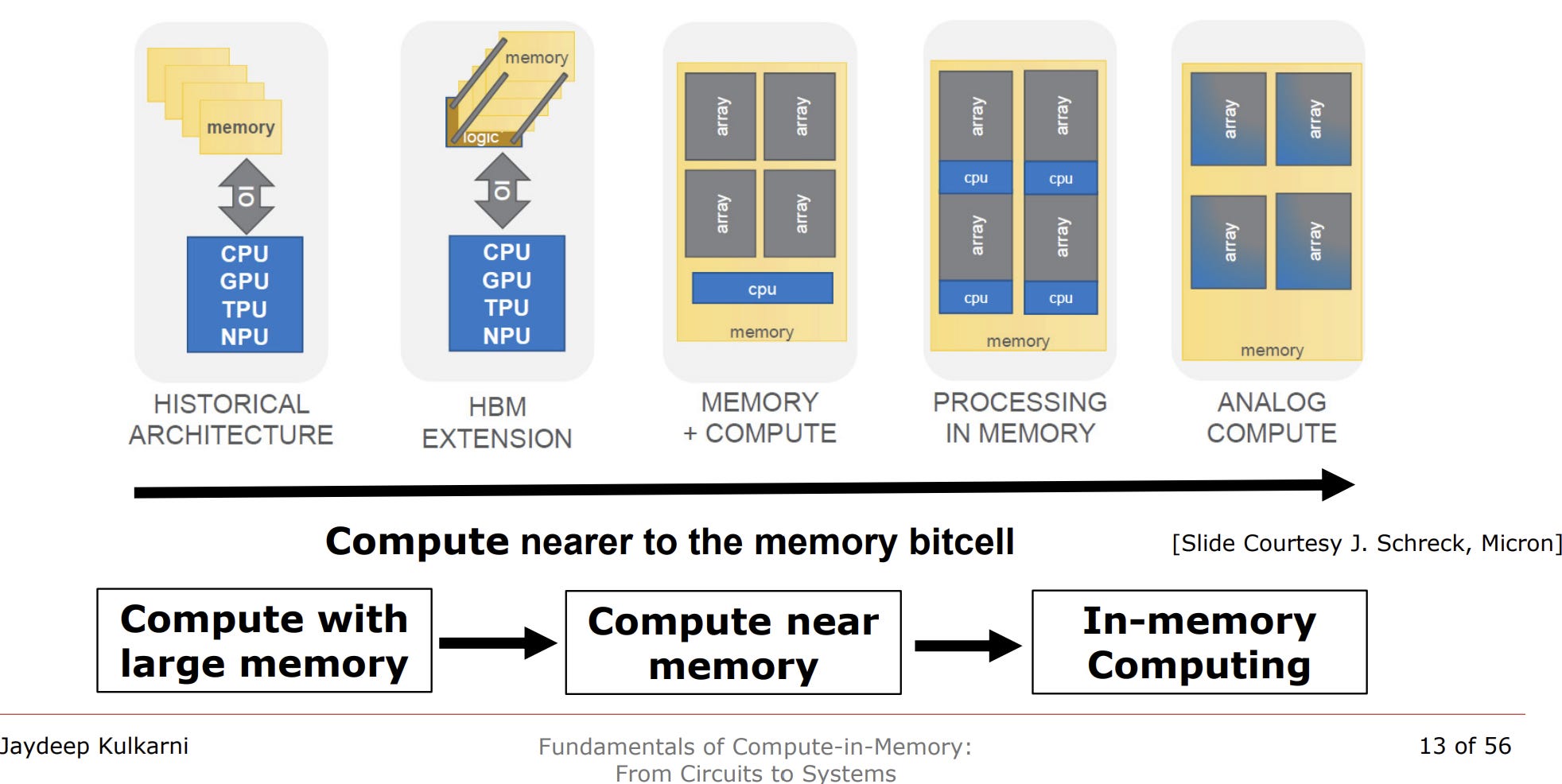
In classical computer architectures, main memory is stored on a huge chunk of off-chip DRAM (HBM) and chunks of data are read onto on-chip caches (typically SRAM) when requested. When MAC operations occur, intermediate results needs to be stored in registers until the final result is computed on.
Depending on how much you read/write data to/from memory, up to 30-70% (or even higher) of the compute energy can from memory transfers, not the compute itself. This makes efforts to optimize / trim data transfers between compute and memory such an attractive option to scale compute efficiency along with performance.
There are three major architectural classifications that classify how close the memory is to the bit cell:
Compute with large memory
Compute near memory
Compute-in-memory
We’ll go through examples within each classification.
Compute with Large Memory
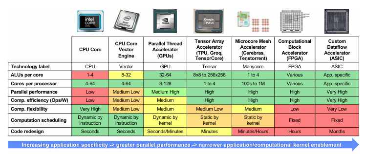
Compute with large memory is the easiest solution to scale in existing paradigms with a large GPU and HBM side by side.
There is a wide range of chip architectures within this compute fabric that vary in specificity and programmability. Most AI accelerators fall in between two conventional categories:
CPUs: Very flexible compute-wise but not optimized for highly parallel inference and training computations.
FPGAs: Used off-the-shelf and easily repurposable for specific embedded applications. FPGAs are preferred for faster time-to-market over custom ASICs since they can be modified with RTL. However, for large models AI, FPGAs are not “programmable” in the SW sense because the hardware effectively changes every time the FPGA is programmed.
The bulk of compute-efficient AI accelerator products lie in-between these two categories to enable software, hardware, and algorithm co-optimization. Two such categories in between fall in the “compute with large memory” paradigm:
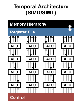
Parallel thread accelerators
Use a temporal architecture with traditional ALUs computed in a SIMT (Single Instruction, Multiple Threads / Data ) paradigm
Typically, one CUDA-thread processes one element of the target data set
All threads in a process share the same memory heap
Key Features
Warp Scheduler - controls a large number of ALU’s by broadcasting a single instruction to all of them to execute in lockstep
Memory Coalescing - combines multiple memory requests from parallel threads into a single, highly efficient memory transaction from the HBM
Memory coalescing is critically important for making data transfer efficient from the HBM
Advantages
Quick to program
The most flexible to handle a wide range of AI applications
Massive parallelism
Disadvantages
Low compute efficiency
Needs sophisticated control circuitry to coordinately data movement across ALUs and memory
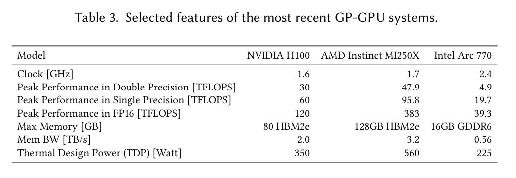
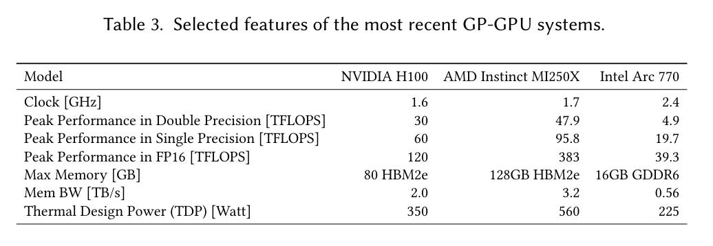
Figure 7. A comparison of general purpose GPU systems. Source: C. Silvano et al. “A Survey on Deep Learning Hardware Accelerators for Heterogeneous HPC Platforms” https://arxiv.org/abs/2306.15552
Examples
NVIDIA H100
AMD Instinct MI250X
Intel Arc 770
Generally speaking, powerful GPUs are used for heavier, general purpose tasks that require large complex models.
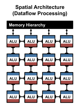
Figure 8. A Spatial Architecture for dataflow processing. Source: V. Sze, Y. Chen, T. Yang, J Emer. “Efficient Processing of Deep Neural Networks: A Tutorial and Survey” https://arxiv.org/abs/1703.09039 Tensor Array
Tensors are mathematical objects that generalizes scalars, vectors, and matrices to higher dimensions
Tensor Arrays use Systolic Arrays or static spatial pipelines. A systolic array is a 2D grid of tightly integrated Processing Elements (PEs) which are a more specialized form of ALUs tailored for MAC operations.
A classic example of one is Eyeriss which I described in more detail in my previous post.
Key Features
Static scheduling - preload model parameters into accelerator before executing inference/training on them
Advantages
Data reuse - data doesn’t have to be stored in registers and can flow between ALUs that perform either Multiply or Accumulate operations
Dense Compute Density
Latency is deterministic - no complexity overhead from unpredictable scheduling
Disadvantages
Rigid, inflexible structure. The array size must be tailored to the specific application
Inefficient at handling sparsity. The sparse data still has to flow through the array
SW compiler complexity
Examples
Google TPU - showcased the first TPU in 2017
Groq LPU
Intel Gaudi
In short, Tensor arrays have the potential to be computationally efficient, but only for specific array sizes.
Compute Near Memory - Manycore
Manycore is an example of compute-near-memory. This architecture decentralizes both compute and memory arrays them along a grid. This shortens the data path from the local SRAM memory to the compute units.
Prominent examples of manycore include:
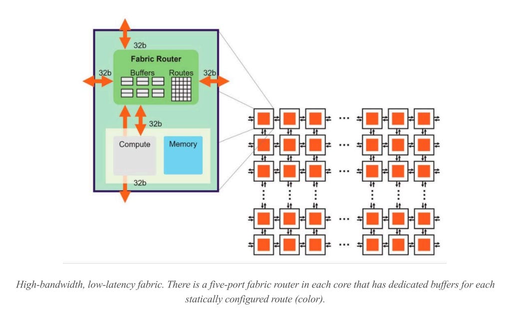
Cerebras
Perhaps the most well-known example of manycore with cores arranged on a wafer scale engine (WSE) with 850k cores
The memory is fully distributed, with the SRAM using 50% of the die area that provides full memory bandwidth to all data paths at full performance, removing the need for data reuse
Their WSE is efficient for sparse matrix operations
Tenstorrent
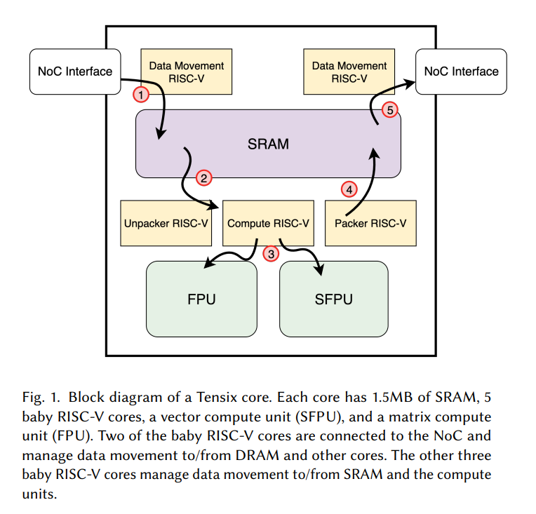
Tenstorrent has a very similar architecture to Cerebras, which fuses a NoC interface to move data to local SRAM to be computed on in each Tensix core.
Advantages
Memory path is short between compute and memory
Disadvantages
Additional software overhead to coordinate data movement to individual cores
Other accelerator options
There are other accelerator options available:
Neural Processing Unit (NPU): NPUs are built specifically to accelerate AI tasks directly on devices like smartphones and laptops
RISC-V processors: RISC-V is a open source ISA widely used among academia and emerging startups. Its modular nature allows easier integration capabilities with embedded applications.
Within the CiM space there are two major categories: Digital, and Analog.
Digital Compute-in-Memory
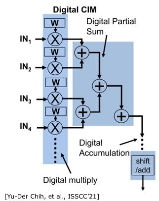
In standard digital PE-based accelerators, the partial sums of the matrix operations are stored in registers and accumulated with PEs. In Digital CiM, these intermediate registers are eliminated and uses digital adder trees after the digital multiply to perform the accumulation of partial sums.
Digital CiM offers the potential to improve energy efficiency MAC operation through bit serial / parallel operations as well as sophisticated control circuits to better control data movement.
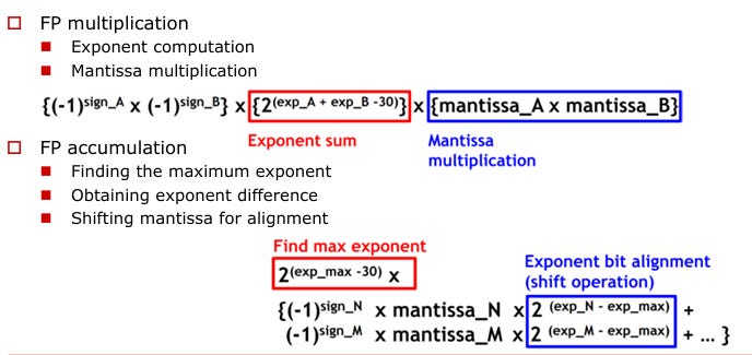
Most efficiency analysis of DCIM is done by examining the intricacies of floating point operations and accounting for the energy consumption of individual operations, which is beyond the scope of this post. In general, with data accumulation trees, the floating point operations need to be synchronized, with a few optimization choices including alignment-first and multiply-first.
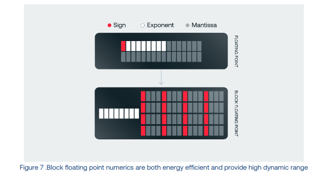
D-Matrix is one of the most prominent examples that leverages their in-SRAM computing techniques. Here they optimize data movement by building SRAM directly into the compute units and use block floating-point math to assign a single shared exponent to a group of numbers.
Despite the promises of digital CiM, there are several challenges with it, a few of which I will discuss after the paywall. I’ll also comprehensively cover the challenges with analog CiM as well.