
APEC 2026: A Complete Overview of the AI Data Center Power System
Why Power Delivery Network Constraints Are Pushing AI Power Delivery Vertical at the Point-of-Load

Editor’s Note (5/26/26): Moving forward, I am transitioning this Substack into a deep-dive resource on System Architecture that covers the packaging, thermal, power, and signal integrity stack. To reflect the depth and combination of the synthesis involved, the deepest technical layers of my guides will now be reserved for paid subscribers.
Before each paywall, I’ll post links to some of my other adjacent posts that give you a well rounded flavor of the interactions amongst other domains.
In this post I cover the following topics:
Core Electrical Constraints of AI Loads
Architectural Goals of AI Power Delivery
Converting below 48V: The many possibilities
🔒Possibilities of 800V to 0.8V Conversion
🔒The Conventional PoL Approach: Lateral Multiphase Buck Converters
🔒Why PDN Constraints Push Regulation Closer to the Chip
🔒Why Vertical Power Delivery Is Emerging as the Endgame
AI compute is scaling so quickly that power delivery is becoming a first-order system bottleneck. Traditional 12V server racks were not designed for AI accelerators that operate at extremely low voltage, draw enormous current, and swing their load profile rapidly.
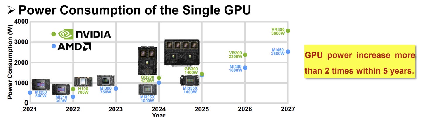
Over the past few years, AI power architecture has evolved quickly, with power demands projected to exceed 1 MW per rack and companies proposing solutions across every layer of the stack. Among those solutions, one direction stands out: vertical power delivery.
Vertical power delivery is emerging as the natural endpoint of a system that must deliver massive current into increasingly power-dense silicon. But that raises a few interesting questions:
How did the architecture arrive there?
What tradeoffs in power distribution make vertical power delivery an increasingly attractive solution at the point of load?
In this post, I build a holistic overview of AI data-center power architecture from first principles to explain why it is evolving in this direction. My aim is to keep the discussion high level enough to provide a map of how the different subsystems influence one another.
Much of the architectures in AI data centers derive themselves from the principles of buck converters. Buck converters are step down DC-DC converters and are the workhorse of most power electronics to bridge the gap between distribution voltage and the voltage that electronics require.
Core Electrical Constraints of AI Loads
Modern AI accelerators are among the most challenging electrical loads because they combine three properties that make power delivery unusually difficult: low supply voltage, high current density, and extremely fast transients.
High power density
GPUs consume massive amount of power due to low supply voltage and very high current:
GPUs operate at very low supply voltage, typically around 0.6 V to 1.1 V. The supply voltage wants to be as low as possible because these devices switch an enormous number of transistors at high frequency, and a lower voltage reduces dynamic switching loss through the familiar P=CV^2*f relationship. Advanced CMOS devices also impose tighter voltage limits because thinner oxides leave less reliability margin. The downside is that at such low voltages, even a small amount of droop becomes significant.
At the same time, GPUs can draw on the order of 1000’s of amps to support massive parallel computation. As compute density increases, the current required to support it rises as well. Since conduction losses scale with I^2*R, every bit of resistance in the path adds significantly more to loss.
Extremely fast transients (up to 2000A/us)
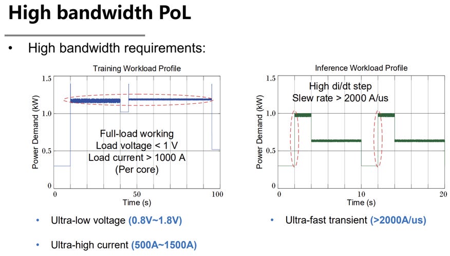
AI loads also exhibit extremely fast transients, sometimes on the order of 2000 A/µs. AI loads can change more quickly than a distant regulator can respond because much of AI computation is performed on-demand through large bursts of multiply-accumulate computations. That forces the regulator and the PDN to work together across a broad bandwidth, often with additional system-level support mechanisms.
Architectural Goals of AI Power Delivery
These electrical constraints force the AI power delivery architecture to optimize around two goals: efficiency and reliability.
Efficiency
Efficiency matters because even a 1% improvement can translate into major savings in heat, electricity, and cooling when multiplied across racks, clusters, and full data centers. That means losses must be evaluated across the entire chain, not just at the converter level.
The converters contribute loss from conduction loss, switching loss, diode-related loss, and CV^2 loss
The PDN contributes additional loss through planes, traces, vias, connectors, package parasitics, and capacitor ESR.
The interconnectedness of the power delivery system is what makes apples-to-apples comparisons across vendors and research papers so difficult. A converter may look excellent on paper, but that does not mean it is the best system-level solution once power density, component count, and PDN burden are considered.
Reliability
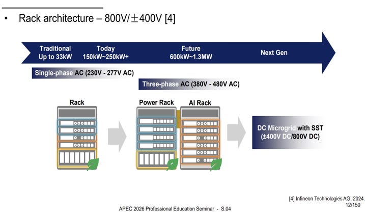
Reliability matters just as much. Data centers make money when they stay online and productive, so the power system must be designed with fault tolerance, serviceability, and safety in mind. As higher distribution voltages such as 800 V enter the architecture, maintainability and safe access become even more important.
Design Goals for the Architecture
The rack architecture for 1 MW-class systems exists to manage current over distance. At a high level, AI power delivery is trying to satisfy two goals at once:
Transport energy efficiently from the power source to the compute load
Regulate it precisely at the point of load.
This is why AI power delivery is fundamentally a distribution-and-distance problem. A data center contains large amounts of compute spread across multiple racks and shelves, and the goal is to move power to each GPU with minimal loss.
That naturally leads to a hierarchical architecture: distribute power at high voltage across longer distances, then step it down progressively as the delivery path shortens and the burden shifts toward precise near-load regulation.
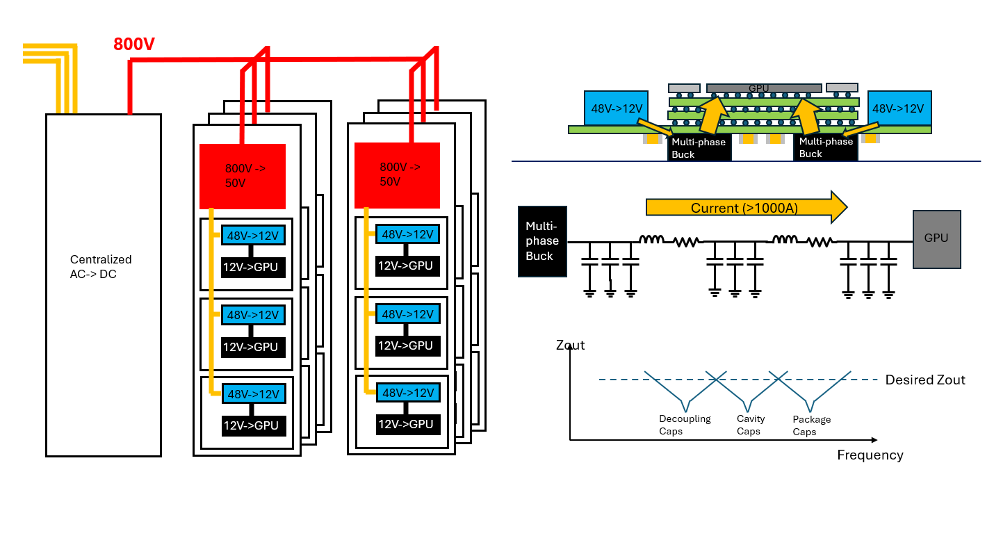
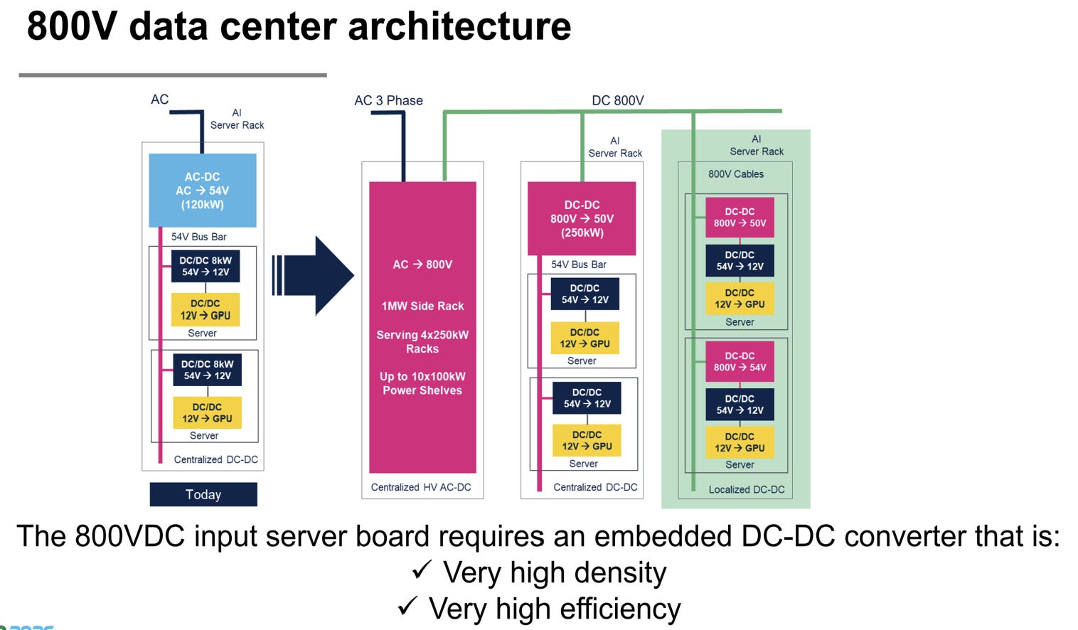
These goals have led to the conventional modular stack: 800V → 48V → 12V → 1V
High voltage minimizes current during long-distance transport amongst racks
48 V provides a practical intermediate distribution rail and minimizes PDN losses within the rack
Lower voltages are introduced only as the distance to the load gets shorter
In short, the architecture tries to keep very high current confined to the shortest possible path near the load itself.
Converting below 48V: The many possibilities
Below 48 V, the design space opens up dramatically because there are many possible ways to reach the roughly 0.6 V to 1.1 V rail required by the GPU.
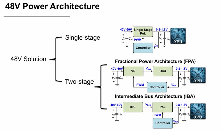
Broadly speaking, these approaches fall into either single-stage or two-stage architectures.
In a single-stage approach, the converter attempts to step 48 V directly down to the load voltage.
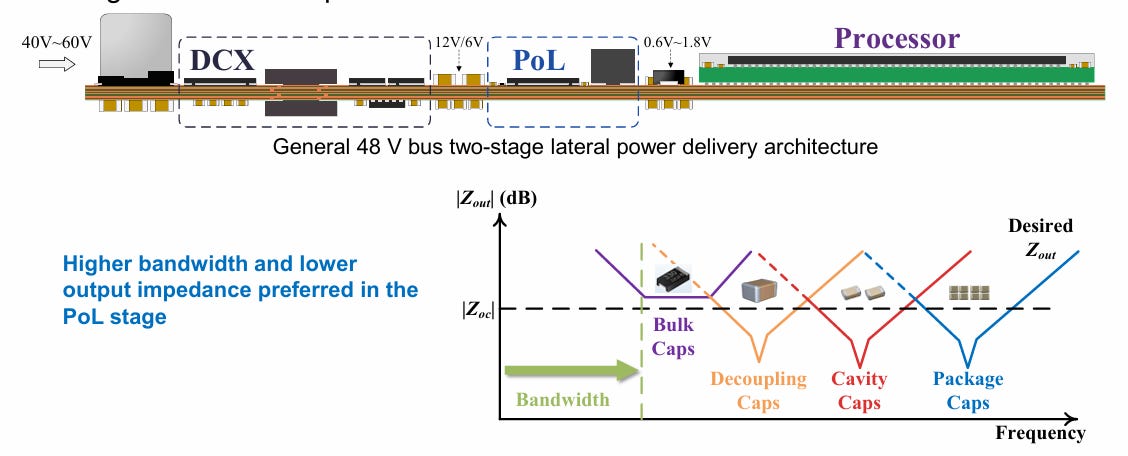
In a two-stage architecture, an intermediate bus converter first steps 48 V down to a lower bus voltage, which is then converted to the final load voltage by a PoL regulator.
The intermediate bus architecture is typically employed because it separates the conversion problem into two more manageable stages in the IBC and PoL. The IBC can focus on efficient transformation, while the PoL focuses on tight local regulation.
Within this architecture there are also commonly employed topologies for both the IBC and PoL and options for the bus voltage:
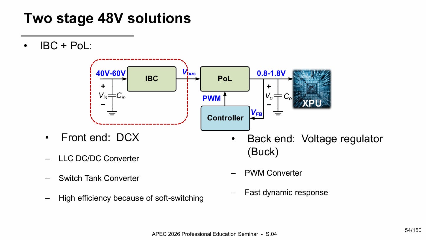
Convert from 48V to 12V and then from 12V to 0.8V. 12V has a very robust server power infrastructure that can be leveraged, so that most engineering effort can be put in the 48V to 12V IBC conversion. This way, researchers can focus on just optimizing on either the 48V → 12V conversion or the 12V→ 0.8V conversion.

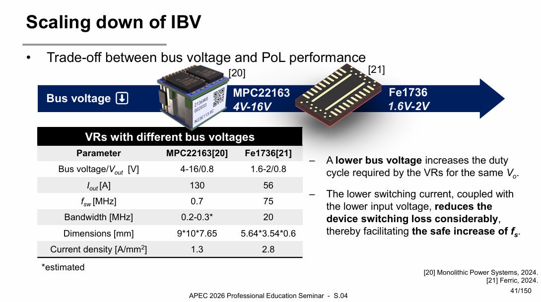
Figure 9. Tradeoff between bus voltage and PoL Performance [1] 
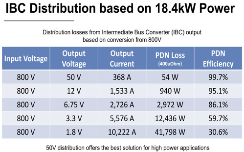
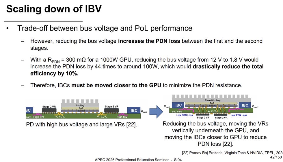
Figure 10. Tradeoff between bus voltage and PoL performance [1] Lower the bus voltage even further from 12V to 6/5/3V. Lowering the bus voltage eases the burden on the PoL since the Vout/Vin ratio is smaller. However, a lower bus voltage also increases the current between the first and second stage, and therefore, the PDN loss between those two stages. This solution pushes the IBC closer to the GPU to minimize PDN resistance, and this in turn pushes the PoL as close to the GPU as possible.
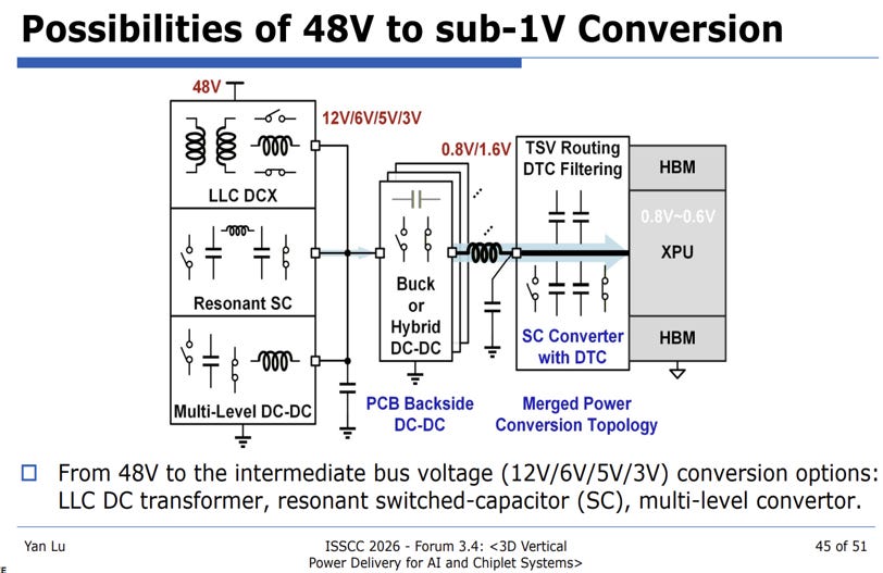
Figure 11. Possibilities of combining two separate converter to create a single unified 48V to 1V converter [6] Convert directly from 48V to 1V. Many research proposals attempt to directly convert 48V to 1V conversion, which typically employ two stage hybrid topologies. This option is very attractive and has a lot of potential, but current solutions don’t always scale to the require current densities and transient responses required.

Possibilities of 800V to 0.8V Conversion
After the paywall I’ll describe the following:
A high level chart possibilities of 800V to 0.8V conversion and PoL delivery options with efficiency parameters
The Conventional PoL Approach: Lateral Multiphase Buck Converters and TLVRs
Why PDN Constraints Push Regulation Closer to the Chip
Why Vertical Power Delivery Is Emerging as the Endgame
If you want to continue expanding your knowledge of the subsystems that underlie power systems, I have a post on the tradeoffs inherent in PMIC design using the buck converter as a design case study.
