
The Phase Locked Loop: A Primer
How PLLs stress high-level, architectural based analog design intuition

Editors note (6/1/26) - Moving forward, I am transitioning this Substack into a deep-dive resource on System Architecture that covers the packaging, thermal, power, and signal integrity stack. To reflect the depth and combination of the synthesis involved, the deepest technical layers of my guides will now be reserved for paid subscribers.
Before each paywall, I add links to additional posts I wrote so you can get a wholistic sense of how systems that interface with PLLs work.
This post covers the following topics:
High level design principles
An Intuitive Look into Type I and Type II Phase Locked loops
Type 1 PLL: XOR and RC LPF
Type 2 PLL: Charge Pump
Bode Plots Comparison for Type I and II PLLs
The Transfer Function of the type II PLL
🔒Common transistor level implementations of type II PLLs
🔒Phase-Frequency detector
🔒Charge Pump
🔒Voltage Controlled Oscillator
🔒LC Oscillator
🔒Current Starved Ring oscillator
🔒Important considerations: Phase Noise and Jitter
🔒A high-level look into the Fractional-N Synthesizer
A modern chip is like a finely tuned orchestra. Each member of the orchestra knows their role and what notes to play, but needs to know when to play them. The conductors role is to align musicians to a shared interpretation of tempo.
Imagine if there was no conductor; musicians don’t know when to play, so the orchestra gets out of sync really quickly as each person plays to their own tempo.
This is the role PLLs play in circuits: as the “conductor” that produces a clock to keep blocks synchronized to a common reference. PLLs help shape and distribute timing under real noise and delays.
The PLL is a beautifully complex and common circuit in ICs that reward high-level analog-design intuition. That is, begin at the architecture level, make sure your design is feasible, and work your way down to transistor level implementation.
At its core, phase locked loops generate clocks from a reference source. This sounds simple, but actually finds use in a wide variety of applications:
Frequency Synthesis: Generate a range of frequency multiples for sampling, DSP, SerDes, RF LO, etc…
Clock Recovery: Recover data from a bit stream of asynchronous data without a clock reference
RF Channel Selection: Select channels across specific frequency channels in transceivers
The question is, why do you need a PLL anyways? Why can’t you just use a reference clock?
Well there are a number of reasons:
Generating internal clocks from a reference- different parts of a system need different internal clock frequencies at different multiples.
Frequency tuning - The PLL frequency can be tuned by controlling parameters
Shaping jitter / phase noise - A PLL “reshapes” noise from a reference source and can be optimized in a way to minimize it. Inside the loop bandwidth, the reference/PFD-path noise tends to dominate; outside that bandwidth, the VCO noise dominates.
Clock skew compensation - In systems with long signal distribution, A PLL can adjust for signal delays across the chip by adjusting its “phase” to be in sync with the original clock.
I want to give a survey level overview of the major design considerations of a PLL at different abstraction levels, from system level, to transistor level, to noise analysis. More detailed information can be found in the book “Design of CMOS Phase-Locked Loops” by B. Razavi [2].
High level design principles
The idea with system architecture is to detect problems at the highest possible level of abstraction.
Typically, at this stage, global stability is owned by the architecture. The architect models the transfer function of the PLL architecture through gain, integrator, and filter blocks.
At this stage there are several things modelled:
Speed - how high are the frequencies needed?
Loop bandwidth and phase margin - how fast does the loop need to be to meet the lock time / overshoot requirements?
Tuning Range - What range of frequencies need to be supported? What VCO gain is required to support this frequency range?
Capture range - What range can the PLL pull-in from unlocked?
Lock/hold range - What is the frequency range over which the PLL stays locked once locked?
Sensitivity - What are the worst case corners with respect to global / random variations? What are critical mismatch sensitivities?
Noise - Where are the major contributors of noise to the output jitter / phase noise?
Spurs - where are reference spurs and fractional spurs?
These issues are investigated in a high level modelling language like VerilogAMS or Simulink.
More local stability issues can be left to transistor level designers like op amp phase/gain margin and gain-bandwidth tradeoffs.
The worst thing you want is to jump to transistor level design with a process and find you can’t implement the frequency or obtain the desired phase noise with the given process!
An Intuitive Look into Type I and Type II Phase Locked loops
The basic idea behind a PLL is that it is a closed-loop system designed to synchronize the output clock to the input reference, whether that be a:
Crystal oscillator
External system clock
Data stream
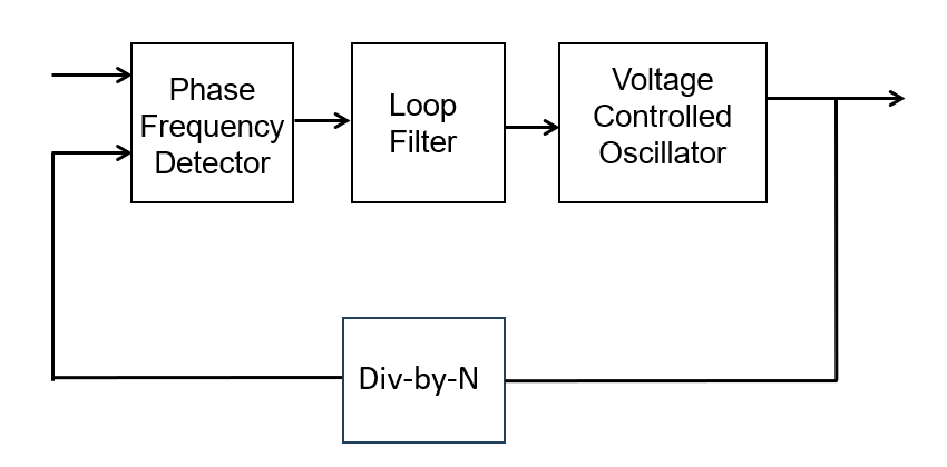
It does this with the following blocks:
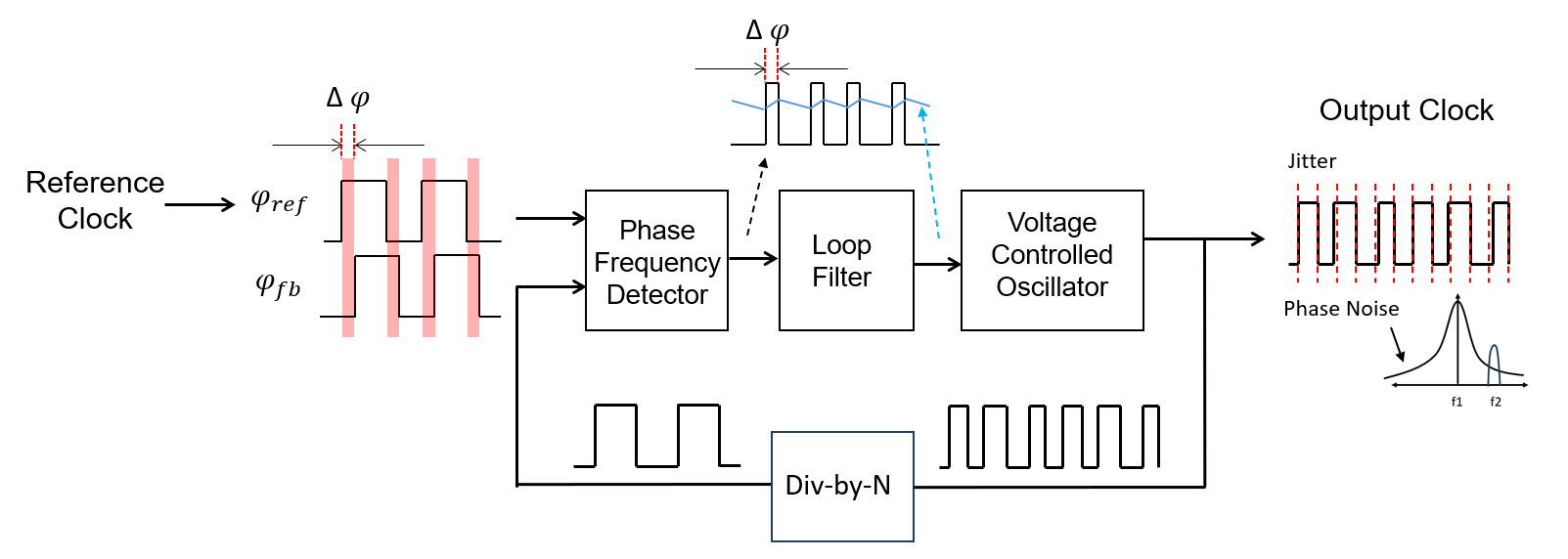
Phase-Frequency detector: Responds to both phase and frequency differences and generates a stream of pulses.
Note that “Phase detector” is used in type I PLLs like in the XOR gate, where the frequencies are already close.
Loop Filter: Filters the input to provide a control voltage Vctrl into the voltage controlled oscillator
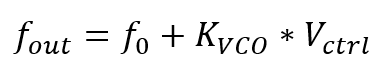
Voltage Controlled Oscillator: Produces an output frequency as a proportion of the input control voltage with a loop gain:

Divide-by-N Counter: Divides the output frequency down by integers of N, allowing the output frequency to be a multiple of the input frequency and the resulting divided clock to be compared against the reference.
The PLL “captures” the frequency from an initial value and adjusts itself until the reference frequency tracks the input frequency. Below is an example of a PLL locking to 7.5MHz in 80us from startup:
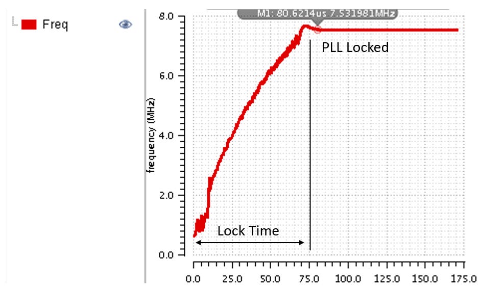
Ideally, when a PLL is in “lock”, the average frequency matches and the phase error settles to a small constant (nearly 0). The voltage on the VCO is a DC value with periodic “ripples” to micro adjust the frequency.
The dynamics of a PLL are similar to damped oscillator systems, with a few different “types” of PLLs:
Type 1 PLL: XOR and RC LPF
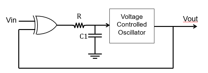
In a simple implementation, one can simply implement the above with an XOR and and RC Low pass filter.
It is type I because it only has 1 integrator:
The VCO
So it has one pole at the origin, and another pole at the RC corner frequency.
However, there are two drawbacks:
Poor lock acquisition - A type 1 PLL often needs the VCO to be initialized close to the target, or else acquisition can be slow or fail without an initialization mechanism
Non-zero static phase error in lock - In lock, a Type I loop typically requires a constant phase offset to sustain the DC control voltage.
Type 2 PLL: Charge Pump
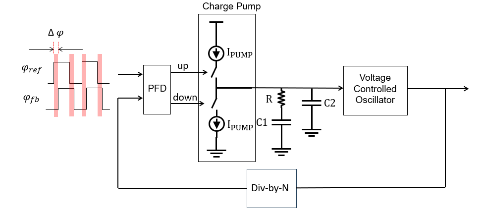
The Charge Pump is a common block used that sources / sinks current into the filter.
Charge Pump PLLs are considered Type II because this system has 2 integrators:
The VCO
The Charge pump current pulses + loop filter capacitor that integrates current to voltage
There are two poles at the origin, and a zero formed by the R.
C2 is added as a high frequency bypass to reduce voltage ripples across Vctrl. C2 is usually smaller, about 1/10 or 2/10 of C1.
Type II integrators can drive steady state error to 0 even with a constant frequency offset, allowing for better tracking and acquisition.
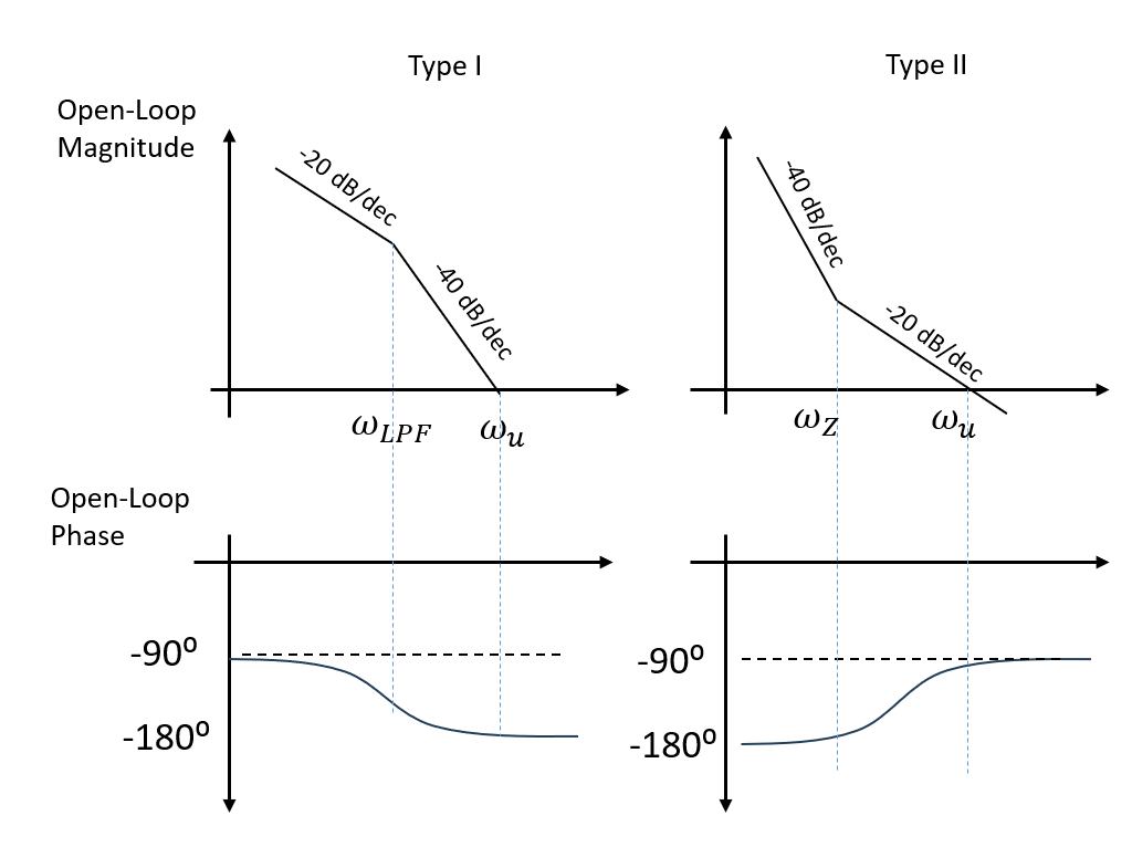
Bode Plots Comparison for Type I and II PLLs
The open loops gains are different for type I and II. Notice how in the type II case, the R introduces a zero that adds phase lead (+90 deg), improving phase margin and stability.
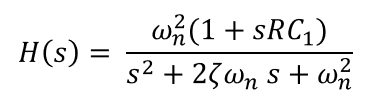
The Transfer Function of the type II PLL
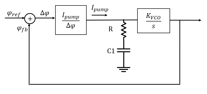
To design a PLL, one must first understand its dynamics through a transfer function. Note that C2 is neglected from this analysis because its value is small compared to C1.
In this derivation, the loop variable is phase, and gains are expressed in the usual PLL units (PFD/CP gain and VCO gain).
The open loop transfer function is given by:
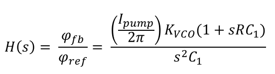
To obtain a closed loop transfer function from an open loop form H(s) and Feedback component G(s):
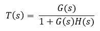
Substituting H(s) into the above:
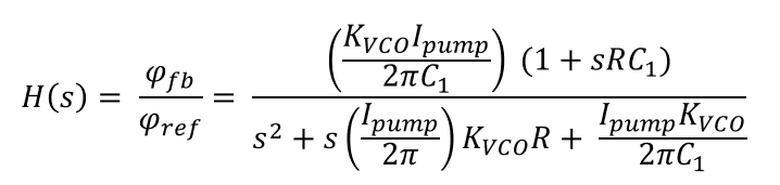
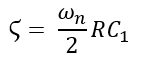
There’s a lot of terms here, but the key thing is that this is a second order transfer function of the form:
With damping factor:
And natural frequency:
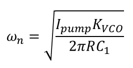
If you recall second order transfer functions, the output “response” can be over or underdamped.
Now that we’ve seen the blocks and built some intuition, we can add additional layers of understanding on top of it. After the paywall we’ll define the common blocks that are used, define where noise and jitter show up, and give a high-level introduction to fractional-N PLLs.
In the mean time, check out my other posts to see the systems that PLLs commonly interface with, as well as how to learn more efficiently:


