
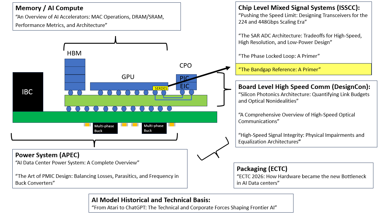
The Bandgap Reference: A Primer
How bandgap references work—and how to design them

Editors note (6/1/26) - Moving forward, I am transitioning this Substack into a deep-dive resource on System Architecture that covers the packaging, thermal, power, and signal integrity stack. I added links to additional posts I wrote that interface with Bandgaps after I originally wrote this one. To reflect the depth and combination of the synthesis involved, the deepest technical layers of my guides will now be reserved for paid subscribers.
However, I’ll leave this post free to get a flavor for the type of depth I go into.
A bandgap reference generates a stable voltage with low sensitivity to temperature, supply, and process (often with trimming).
Most IC datasheets specify that the IC will work within a specific temperature range (such as -55 ̊ C to 125 ̊ C). Variations in temperature can shift bias points and thresholds enough to break specs without a stable reference and proper matching.
Bandgap references are found in virtually all analog circuits as stable references for high-precision analog functions, such as ADCs, DACs, and comparators. They are also used to bias current mirrors for setting bias points so that the resulting circuit is robust to PVT variations. Because of their ubiquity, they tend to be reused and modified depending on the fab process and the level of precision required.
Bandgaps look simple, but are a delicate balance of a few fundamental analog principles, including:
Matching: resistor ratios, BJT area ratios, amplifier offsets
Feedback: Forcing ΔV_BE and setting I_PTAT robustly
Temperature variation: How BJT and resistor characteristics vary over temperature, sometimes nonlinearly
Trim & Calibration: Output accuracy, temp trim, and curvature correction
Below is a self-biased bandgap design example I built that illustrates these principles. I also have a fun side story at the end about how a group of young designers “competed” on who can make the best bandgap.
Circuit Analysis
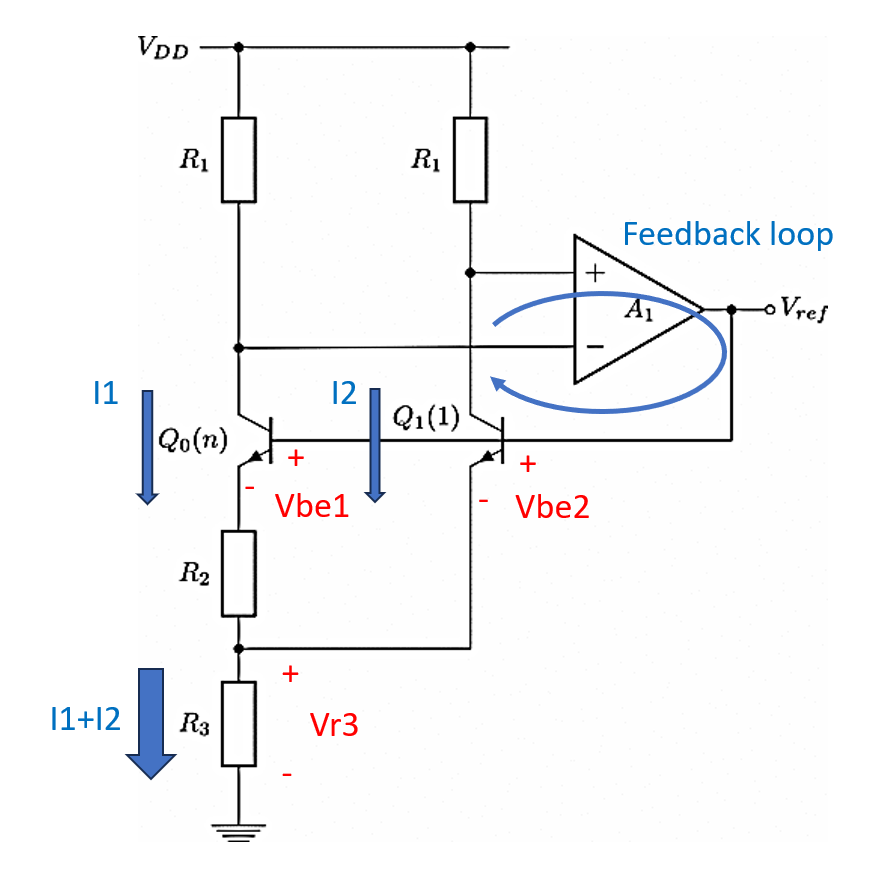
Consider the Brokaw Bandgap reference in Fig. 1. The reference voltage is the output of the op amp. This circuit sums a PTAT voltage and a CTAT voltage:
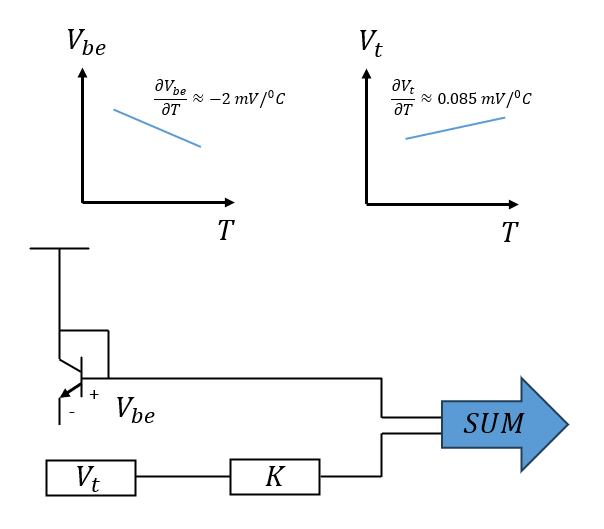
A PTAT voltage (Proportional to absolute temperature) means that the voltage increases with increasing temperature.
The PTAT voltage is generated by the BJT base - emitter voltage difference ΔV_BE = Vt*ln(n) by forcing two BJTs to operate at different current densities (often via an emitter-area ratio n). This voltage appears across R3 in the above example.
A CTAT voltage (Complementary to absolute temperature) means that the voltage decreases with increasing temperature.
The CTAT voltage is generated across the base-emitter of the BJT which behaves like a diode. The reason behind this is related to the fact that the bandgap energy of silicon decreases with increasing temperature.
Additionally, the op-amp sets the PTAT current by driving the loop so its input nodes match (in the ideal case).
When both PTAT and CTAT voltages are summed with the right scaling, the first-order temperature dependence largely cancels, leaving a much flatter reference over temperature.
Derivation of Output Voltage
The derivation of the output voltage is as follows. Starting from KVL:
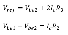
The current through the circuit flows through R2, where the voltage across it is the difference of the base-emitter voltages of Q and Q1:
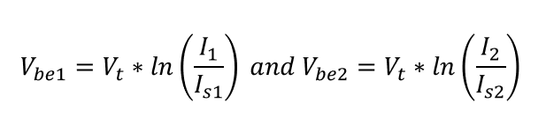
Is is the saturation current of the diode. Substituting all of the terms:
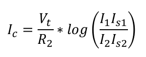
The op amp uses negative feedback to ensure that I1=I2, so both terms can be cancelled. However, Is1 and Is2 are proportional to the cross sectional area of the BJT. Therefore,

where n is the number of BJTs in parallel for Q0. The output voltage is given by:
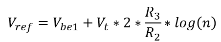
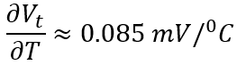
The output voltage is the sum of a PTAT voltage (Vt) times a gain term and a CTAT voltage Vbe1. However, the temperature variations are not the same. The temperature variations of each term are:
The values in the term R3/R2*log(n) are selected such that the dV/dt of both terms cancel each other:
n = 8 is common because 8 unit devices plus 1 unit device can be arranged symmetrically (e.g., a 3×3 array) to improve matching.
The resistor ratio R3/R2 is selected to be equal to 5.5.
Using a bias current of 55 uA and Is1 = 6.734 fA from the SPICE model, and substituting all of these values in the equation above:
Vbe1 = .59V.
Vref at 27 °C = 1.18V.
Circuit Schematic and Simulation Results
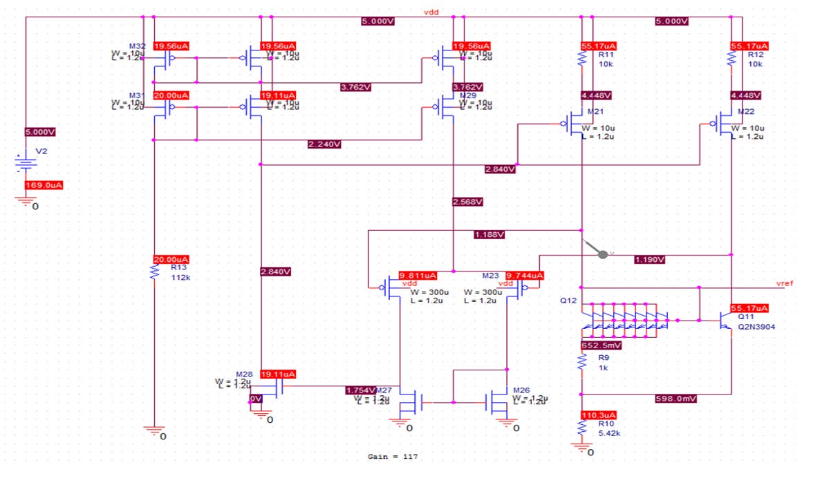
The circuit consists of the bandgap core which generates the PTAT and CTAT voltages. Both collector voltages are fed into an op amp which uses a PMOS differential pair as the first stage. This is done to avoid the VMIN problem an NMOS based op amp would experience since the common mode input voltage is approximately 1.18V.
The output of the first stage is fed into a second stage where the output is referenced to the VDD rail to control the PMOS current sources. The op amp is biased with a PMOS based cascode current mirror of 20uA. All of the DC voltages and currents are shown at T = 27 °C.
The simulation results of the bandgap reference are shown below.
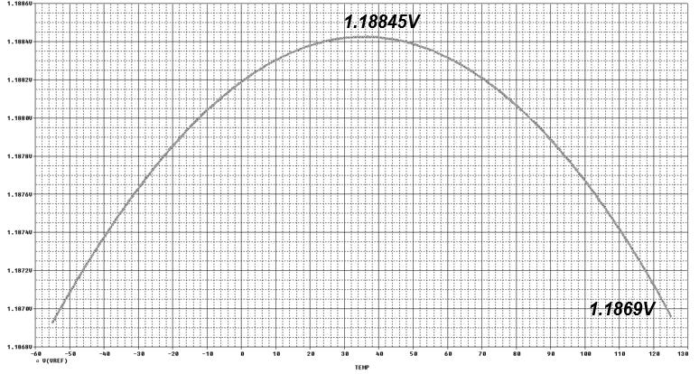
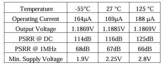
Output voltage across temperature. The graph above shows the DC value of Vref as temperature swept from -55 °C to 125°C in 1°C increments. Ideally, the voltage should be flat across temperature, but the simulation shows the voltage follows a parabolic shape. The maximum voltage is 1.1885V which occurs at approximately 30 °C. The voltage drops for lower and higher temperature, where the minimum voltage is approximately 1.1869V. When the voltage is confined to this range, the maximum voltage difference is 1.6 mV, which is a variation of 0.14% over temp.
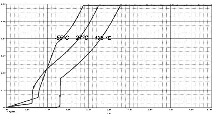
Line Regulation. This simulation sweeps the value of the voltage supply for three different temperatures: -55 °C (left curve), 27°C (middle curve), and 125 °C (right curve). The reference voltage stabilizes when the power supply has reached a certain threshold. This threshold is different for all three temperatures and is shown in Table 1. Once the power supply voltage has reached its threshold, the reference voltage is fairly stable.
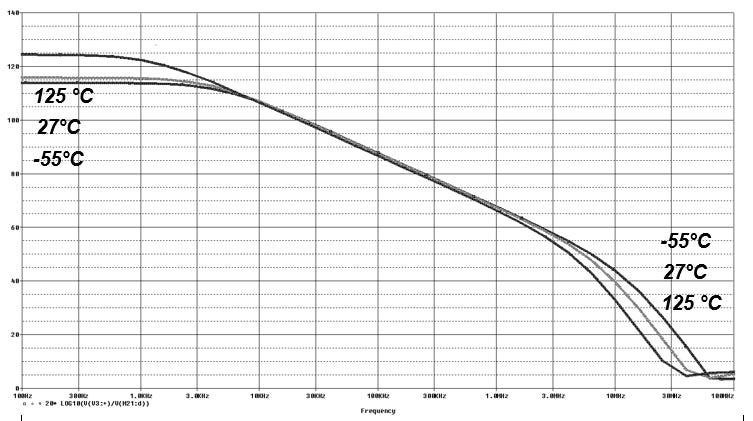
Power supply rejection ratio, or PSRR. The PSRR is the ability for the circuit to reject noise from the power supply. It is defined as:

To perform this simulation, an AC signal of 1 mV was places in series with the power supply voltage. An AC sweep was performed for three temperature values from 100Hz to 100MHz and the magnitude of the output voltage was observed. The above formula was then applied to obtain the plots shown above, with results shown in table 1.
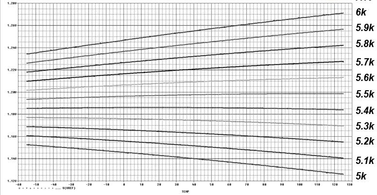
Mismatch in R10 Resistor. The resistance was swept parametrically from 5kΩ and 6kΩ in 100Ω increments and the output voltage is plotted. This simulation shows that for low resistor values, the CTAT voltage of the BJT dominates the characteristic, and the curve drops over temperature. When R10 is high, the PTAT voltage dominates, and the reference curves increase over temperature.
The following chart summarizes the simulation results.
Additional Features
There are additional features that bandgaps need:
Trim Range. The degree to how precise a bandgap has to be depends on the precision required across PVT. Monte carlo simulations are run to determine the untrimmed range over which the output voltage can vary, and trim features are added in appropriate places to ensure the output voltage can be turned to within spec across the temperature range.
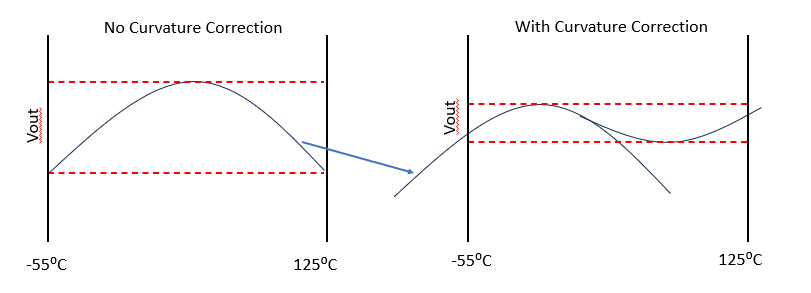
Curvature Correction. Parts that operate in wide temperature ranges with tight specs can require additional “curvature correction” to improve the error across temperature. First order cancellation like resistor-only tuning can give residual curvature because parameters can have nonlinearities across temperature (such as BJTs) that affect the output.
Startup Circuitry. Because the core is self-biased, it has a zero-current equilibrium point, so startup circuitry is required to guarantee the intended operating point.
Story time: A Friendly Bandgap Competition
At an Analog Design internship, I once saw a group of young engineers have a friendly completion against each over who can design a bandgap with the highest accuracy across temperature. Work was to be done after 2-3pm on Friday so as to not interfere with day to day work.
Most of the “tricks” they experimented with involved:
curvature correction techniques, like how to bias a transistor to turn on as a specific temperature, and where to place in the circuit
NPN / PNP topologies
value ratios (n, resistors)
what current mirror to use (cascode, wide swing, source degenerated, wilson)
what amplifier topology (NMOS, PMOS, gain stages, active loads) maximize gain and minimize offset
Each participant presented their results weekly and learned insights from each other to improve their day job, since analog is an art after all.
Conclusion
I feel like designing bandgaps are a really good introduction to analog circuit design because designing them develops a lot of the fundamentals used in more complex analog circuits.
If you’re curious about how bandgap references are used in higher level systems, check out my other posts here:


References
[1] Timm, S. Wickmann, A., “A Trimmable Precision Bandgap Reference on 180nm CMOS”, Semiconductor Conference Dresden-Grenoble (ISCDG), 2013 International, 26-27 Dept. 2013, http://ieeexplore.ieee.org/xpls/icp.jsp?arnumber=6656292
[2] Hugo. “Bandgap voltage Reference” [Online]. Available: http://www.onmyphd.com/?p=bandgap.reference
[3] P. Miller and D. Moore. (2005). “Precision voltage references” [Online] . Available: http://www.ti.com/lit/an/slyt183/slyt183.pdf\
[4] A. Paul Brokaw. (2011). “How to make a bandgap reference in one easy lesson” [Online]. Available: https://www.idt.com/document/whp/how-make-bandgap-voltage-reference-one-easy-lesson-paul-brokaw