
The Art of Power Management: Balancing Losses, Parasitics, and Tradeoffs in Buck Converters
Why competing tradeoffs in buck converters make it one of the most competitive markets in the semiconductor industry

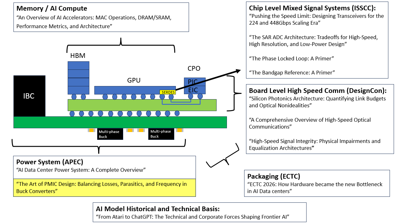
After traveling to four flagship semiconductor conferences (ISSCC, DesignCon, APEC, and ECTC), its clear that the intersection of high speed communications, power, packaging, and thermals where the real architectural bottlenecks are happening.
Moving forward, I am transitioning this Substack into a deep-dive resource on System Architecture that covers the packaging, thermal, power, and signal integrity stack. I added links to additional posts I wrote that interface with Buck converters after I originally wrote this one.
To reflect the depth and combination of the synthesis involved, the deepest technical layers of my guides will now be reserved for paid subscribers.
However, I’ll leave this post free to get a flavor for the type of depth I go into.
If you want the full bird’s-eye view of how these systems fit together, consider upgrading to a paid subscription.
Buck converters are where the money is, especially in AI data centers, because most electronic systems need some form of step down conversion.
Buck converters are a DC-DC converter responsible for stepping down voltage from a higher voltage to a lower one. They are often times the chips at the “Point of load” (PoL) after AC rectification to an intermediate voltage. In most electronic systems, distribution voltage tends to be high (like 2-4S Li-ion batteries and 48V busses) and required chip voltages are low, (especially in advanced process nodes that can run anywhere from 0.5V-1V).
Buck converters are becoming increasingly challenging to design as distribution voltage gets higher and process voltage gets lower. High efficiency, precise control of control loops, and component area become increasing important as PMICs tend to be highly tailored to the specific application it is powering.
In this post, I want to provide a look into the fundamental operation of the buck converter and how nonidealities affect performance. I’ll cover continuous conduction mode power stage fundamentals. Control-loop design, DCM modes, EMI compliance, and advanced architectures (3L, Multiphase) are intentionally out of scope and left for a future post.
Much of this information is synthesized from the book “Design of Power Management Integrated Circuits” along with my original insight; refer to the book for more details.
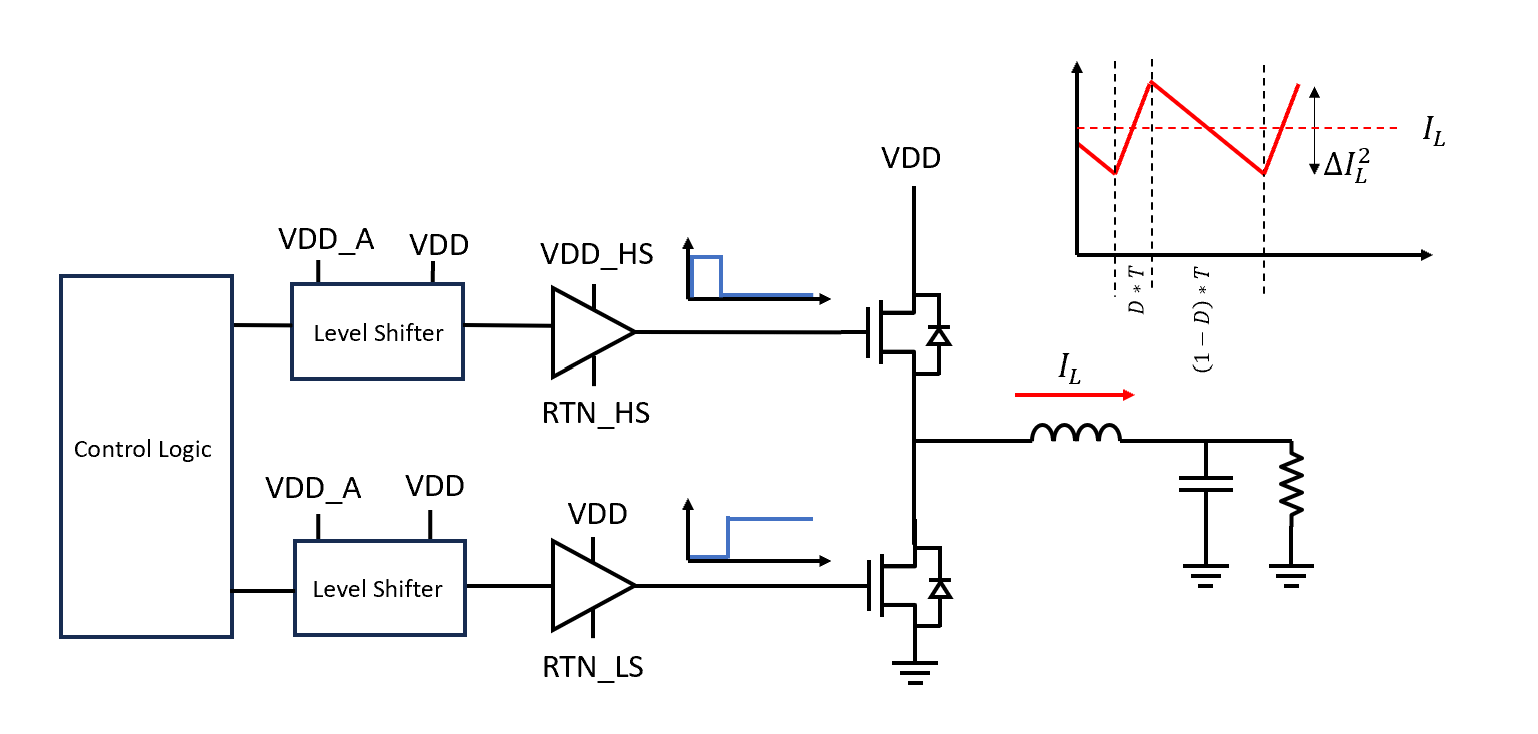
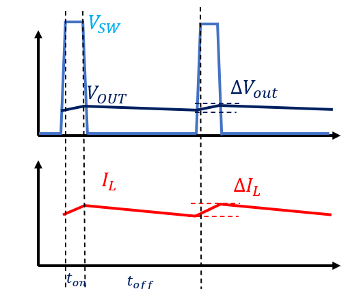
The buck converter in CCM: principle of operation
To begin, we look at the inductor current during two time periods: t_on, and t_off
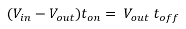
t_on: Energy is charged through the inductor:
t_off: Energy is discharged from the inductor:
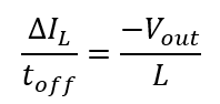
During steady state operation, we need the voltage across the inductor to average out to 0 over time. Therefore, we need the change in current during t_on equal the current going out on t_off. Setting delta_Il equal to each other and arrange terms we get:
Rearranging terms to get the voltage conversion ratio:
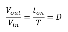
There are two important quantities here:
Current Ripple
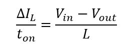
The current through the inductor will ripple as it is switched on and off. The delta in the current ripple is given by:
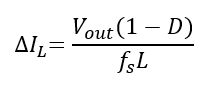
The variables should be selected to make the current ripple reasonable. As a general rule of thumb, current ripple is typically +- 20%. Note that this is not the same value as the voltage/load current ripple since the current ripple gets “filtered” out to be much smaller.
Voltage Ripple
Due to the switching and filtering operation inherent to DC-DC converters, the output will experience a small amount of voltage ripple:
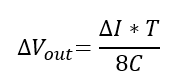
The capacitor value and switching frequency should be selected to ensure the voltage ripple is within the desired specs.
How Nonidealities and Sources of Loss affect efficiency
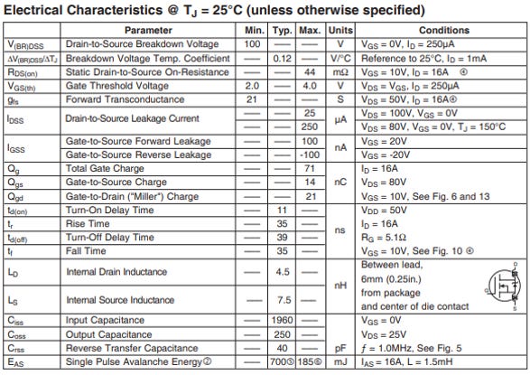
All electronic components have important nonidealities that contribute to loss. MOSFETs have a few important nonidealities worth pointing out:
Gate Charge. Charge accumulates on the gate of the MOSFET to be able to turn this on, typically in the nC range. Note that gate charge and energy dissipated are usually specified rather than power, because actual power loss depends on the switching frequency selected by the designer.
R_dson. The resistance of the MOSFET in the ON state. Lower is better.
Turn on / off Time. The time it takes for the switching nodes to transistors to ON/OFF.
Parasitic Inductance. The parasitic inductance of the MOSFET due to packaged leads. Parasitic inductance can have an impact on ringing/EMI/overshoot that can be mitigated by making loops tight.
Input / Output Capacitance. The terminals of a MOSFET have capacitance that direct affect how fast the nodes can be switches on and off.
These nonidealities lead to a few major sources of loss that direct affect efficiency: Conduction, switching, diode, CV², gate driver, and supply-related:
Conduction (I²R) losses
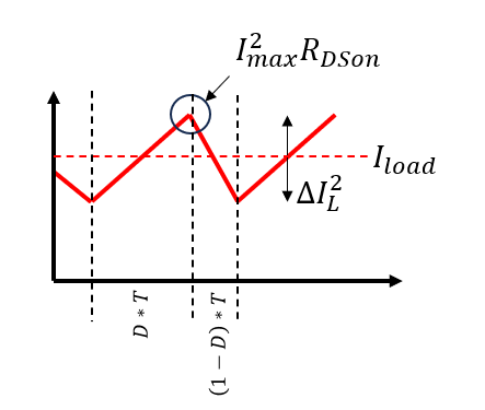
Conduction loss occurs due to the IR drop across the MOSFETs Rdson during steady state operation. For a single transistor switching, if Iload is fairly flat, the conduction loss is equal to.
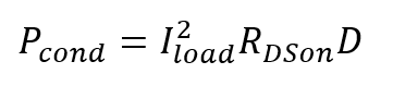
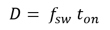
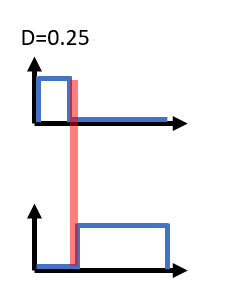
Where D represents the duty cycle, representing the % time the signal is high and the switch is on:
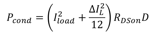
However, large current ripples increase conduction loss because this loss scales with I², so the moments where I is higher than average causes it to burn more power that when the current is lower than average. This is accounted for as a delta_Il term:
Switching losses
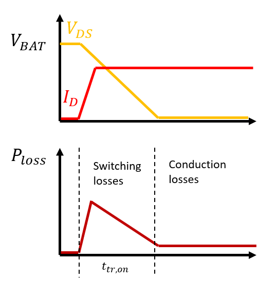
Switching losses occur when switching between ON and OFF as there is a region in which Vds is decreasing as Id is increasing. The loss of this region is given by:
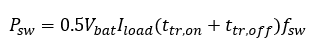
There are two notes here:
This loss scales with switching frequency. As you switch at a higher frequency, the switching loss increases since there are more triangle regions where energy is dissipated.
This waveform applies to the “hard” switch case where the voltage across the switch is not 0 when it is turned on. “Soft” switching technique attempt to reduce this voltage through techniques like resonant circuits to switch at Zero voltage (ZVS) or zero current (ZCS).
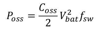
CV² Losses in the switch nodes
There is power dissipation due to charges when the switch node is capacitively charged up through the input voltage:
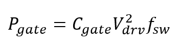
Charge Losses in the Gate driver. This is caused by the charge required to drive the gate of the MOSFET high to be in the “ON” state:
Diode - related losses.
The diode in figure 7 has two losses associated with it.
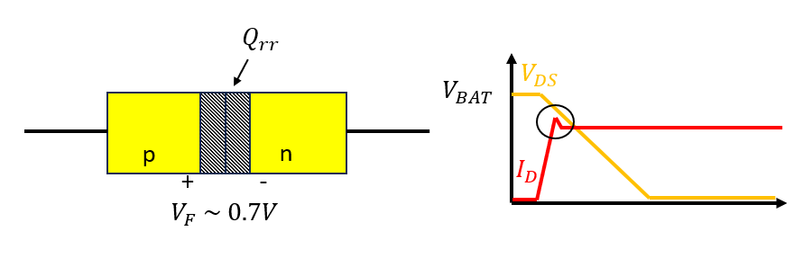
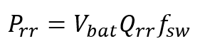
Diode Reverse recovery. Reverse recovery is an effect in pn-junctions in diodes (and MOSFETS as well) where charge Qrr is required to bring diode D from ON to OFF. This charge also rushes out and is seen as a tiny “blip” in the voltage waveform. This effect has a finite amount of time, and its loss is given by:
Diode Conduction loss. When the current conducts through a diode, it experiences a forward voltage drop Vf and the loss is given by:
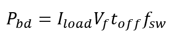
This loss is important to consider when dead time is discussed.
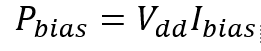
Supply Current related losses
The housekeeping and control circuits on chip itself will consume power to maintain operation:
This current draw can change depending on the state of the device (shutdown, standby, full operation, light load operation) and should be properly quantified on a datasheet to ensure there are no unexpected power leaks in the chip.
Sidebar - The Miller Plateau - Switching a single transistor
One note about switching is that is NOT a linear ramp, but rather there is a plateau that the gate voltage sits that directly affects rise / fall times.
In the resistive load case, there are three phases of switching:
T1: Precharge phase. Enough charge accumulates on the gate to turn the transistor on when Vth is reached
T2: Miller phase.
At the input, Vgs rises slowly due to the miller effect
At the output, Id begins to rise and Vds falls
T3: End of Miller phase. Id has reaches its peak value to supply Rload, so VGS is able to increase to its maximum value
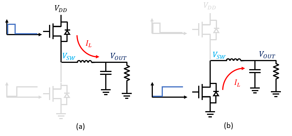
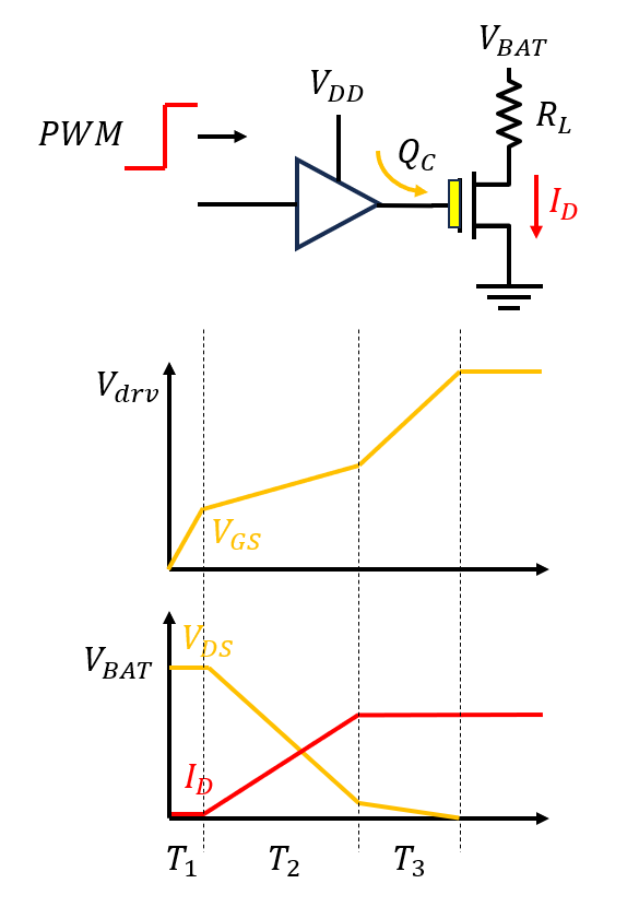
Lets extend these concepts to inductive loads, which is what most buck converters switch into. Note that this switching diagram assumes the inductor current is at steady state at time T0.
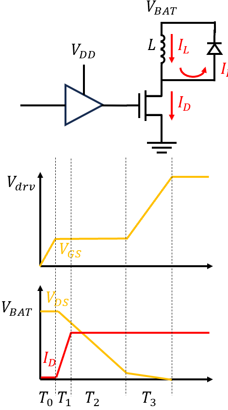
In the inductive load case, there are three phases of switching:
T1: Beginning of Miller phase. Id ramps up quickly to take the inductor current As the switch is turned on, Vds begins dropping
T2: Miller Plateau. Vgs stays in the miller “plateau” until Vds continues dropping until it hits 0
T3: End of Miller phase . Vgs continues to reach its maximum value.
Tradeoffs
The buck converter looks simple, but in reality, buck converter design is an art due to the sheer number of interactions and tradeoffs that designers must make. Lets take a look at a few:
Switching frequency vs component size / frequency dependent losses / EMI
Increasing the switching frequency is desirable for a few reasons:
Current ripple decreases
Lower component values can be used since there is less on and off time
However, there are a few undesirable effects:
Frequency-dependent losses increase (Switching, CV²*f)
EMI increases
Therefore, an preliminarily loss across frequency analysis needs to be performed to select an appropriate switching frequency that balances performance and losses.
Dead time vs diode loss
Both switches must avoid being turned on at the same time at all costs for obvious reasons. To prevent this, a feature called “dead time” intentionally adds in a small amount of “off time” between switching cycles to guarantee that both switches will not be on at the same time.
However, during this dead time, the current has to flow through the diode of the low side FET to maintain continuous current through the inductor. This adds loss.
A small amount of deadtime is desired, but should be not too large to make the conduction loss through the diode a major loss source.
Trace and Package Parasitics
Parasitics have important implications during layout because your circuit can look like unintended LRC circuits if parasitics aren’t well controlled. Uncontrolled parasitics can result in a bunch of nasty interactions and effects such as ringing that can cause overvoltage conditions as well as diodes forward biasing. Parasitics include the following:
Parasitic Inductance. Large current area loops have a lot of inductance. Bond wires in discrete transistors have inductance due to the area underneath the bond wire where magnetic field flows that resists changes in current.
Parasitic Capacitance. Virtually every node has a capacitance where the voltage on a node is maintained with charge with a ground reference.
Parasitic Resistance. Parasitic resistance shows up current carrying metal that can affect IR drop, as well as the Equivalent Series resistance (ESR) of the output capacitor
Parasitics should be added as early in the modelling process and simulated with PEX at the end to ensure proper circuit functionality.
Conclusion
Buck converters look simple on paper—two switches, an inductor, and a capacitor. But in reality, buck converter design is an art. Hardware, efficiency and stability are negotiated between switching losses, ripple, dead time, and parasitics. And that doesn’t even include the complex control schemes and advanced architectures that performance-defining products need.
That’s why PMICs aren’t one-size-fits-all: the “best” buck is the one customized to its system’s voltage range, load dynamics, noise tolerance, and thermal limits. As a result, PMICs tend to be a very competitive industry with marketing managers claiming they have the best “bang for your buck”. No pun intended :)
If you want to learn more about buck converters used in the power system of AI data centers, especially multi-phase and TLVR variants, check out my other post on “AI Data Center Power System: A Complete Overview”
AI Data Center Power System: A Complete Overview

AI compute is scaling so quickly that power delivery is becoming a first-order system bottleneck. Traditional 12V server racks were not designed for AI accelerators that operate at extremely low voltage, draw enormous current, and swing their load profile rapidly.