
ECTC 2026: The Multi-Physics and Packaging Bottlenecks of Next-Gen AI Clusters
Key challenges in Advanced Packaging, Reliability, CPO, and Multiphysics simulation

Editors Note (6/22/26) - I am paywalling the last half of this post. Before the paywall, I link several of my other posts in adjacent domains in power electronics, high speed communications, and signal integrity that related to packaging in some way.
In this post I discuss the following topics:
Clear definitions of five buzzwords used in advanced packaging from John Lau’s tutorial
How Reliability is one of the biggest concerns for engineers on the floor
🔒The Wild West of Co-packaged optics - Different CPO Integration Options
🔒Why Multiphysics simulation is not that easy in practice
Hardware is becoming the new bottleneck in hyperscalers.
That was was the underlying message at ECTC 2026, the flagship electronics packaging conference, as stated in a plenary session by Dr. Tien Wu, CEO of Advanced Semiconductor Engineering, the largest OSAT in the world.
I attended ECTC 2026, not as a pure packaging engineer, but as a Analog/Mixed signal system architect who is curious about how advanced packaging is interrelated with other elements.
Before I came to this conference, I went in knowing a bit about advanced packaging from other writers. I studied mixed signal architectures in high-speed communications and power systems through self-directed conference travel to ISSCC, DesignCon, and APEC. I wrote comprehensive architecture breakdowns specifically to bring awareness to key constraints so that engineers can ask more informed questions earlier in the design process. I wrote about why I am doing this in my post:

As an EE myself, we sometimes take packaging for granted. However, ECTC made me realize the sheer amount of depth and mechanical considerations that go into packaging. The performance demands of GPUs are placing a lot of stress on the packaging itself and shifts the bottleneck toward hardware, not software, as the limiting factor in scaling AI compute performance.
In this post I’ll give a very broad high level overview of my experience at ECTC and the key challenges engineers on the floor are facing.
John Lau Tutorial on Advanced Packaging
At the beginning of the conference, I acquainted myself with advanced packaging trends through a tutorial given by John Lau. He is considered a legend in the packaging community because he wrote virtually every major book on advanced packaging and heterogeneous integration. He is very practical and as close to the manufacturing reality. His lecture was an experience; he tends to “beat” concepts into your head through repetition; I am not joking. I felt like I passed through a rite of passage.
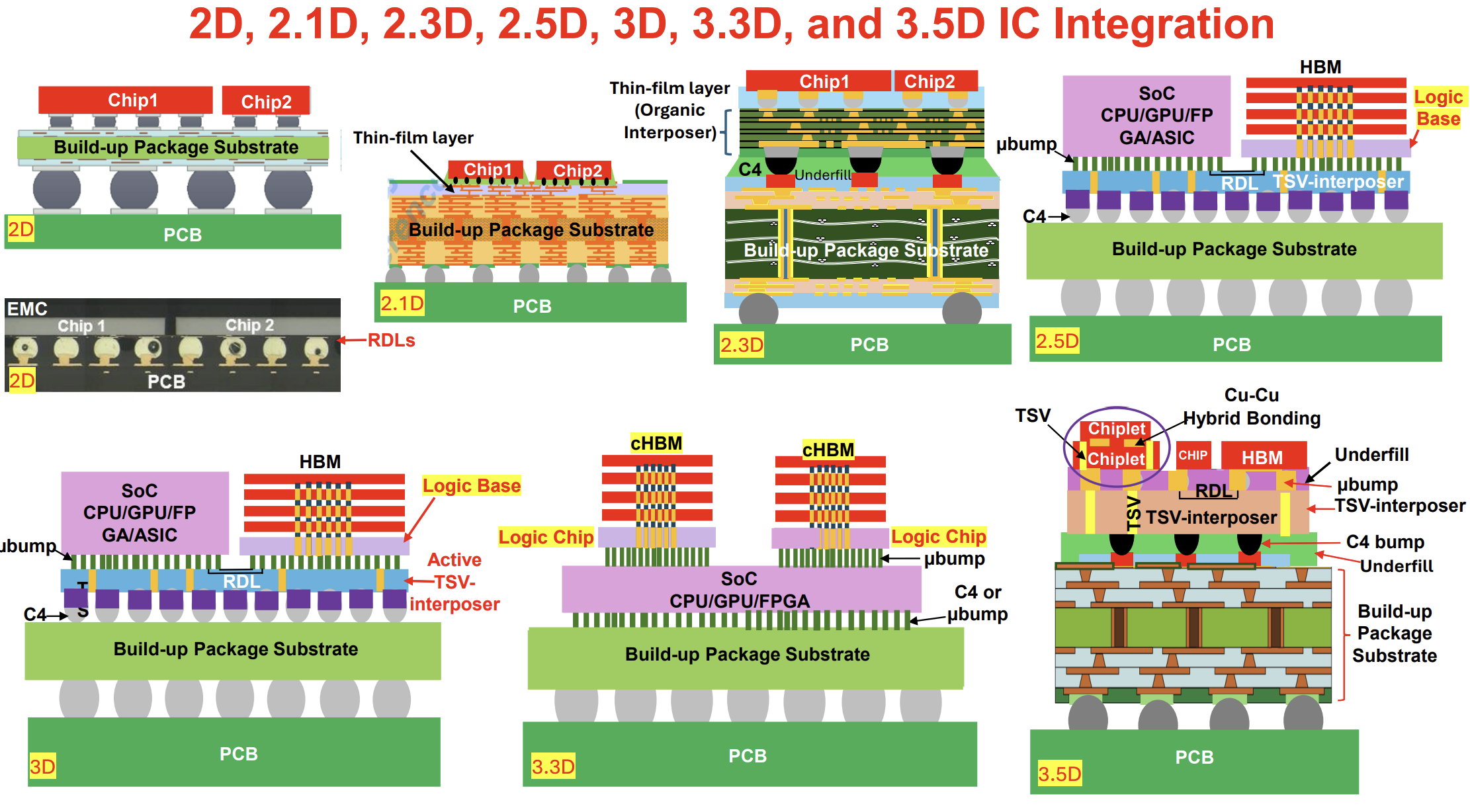
He broke down the classifications (2D, 2.1D, 2.3D, 2.5D, 3D, 3.5D) as shown in the figure above, as well as described key issues in hybrid bonding and glass substrates. These topics are covered quite extensively by other writers and I will not go into depth here.
He notes that several terms in advanced packaging are often misused. He clearly defines these terms as the following:
Chiplet is a Chip Design Method
Heterogeneous Integration is a Chip Packaging Method
Photonic Devices - components that generate, manipulate, and detect light (LED, Laser, etc)
Silicon Photonics - a technology that integrates optical components onto a silicon chip, enabling the transmission of data using light instead of traditional electrical signals. Si Photonics is the semiconductor integration of PIC and EIC on a silicon substrate (wafer) with CMOS (complementary metal-oxide semiconductor technology)
Co-packaged optics (CPO) - a heterogeneous integration packaging method to integrate chiplets, including the optical engine, electrical engine, and an ASIC switch.
He is also well versed in the second-order effects of manufacturability. He mentioned how larger panel sizes (600x600mm) that pack more parts per panel are not always better because it takes longer for the pick and place machine to traverse the distance to move the parts between panel and product.
After the seminar, I personally ordered up a book myself “Hybrid Bonding, Advanced Substrates, Failure Mechanisms, and Thermal Management for Chiplets and Heterogeneous Integration” (2025) to understand the interactions between advanced packaging and adjacent domains. I anticipate this book will strike a balance in describing the interactions with advanced packaging with other domains and will be a valuable resource. I’ll use the material in this book to inform my future writing.
In my view, there is a ton of noise and hype around advanced packaging. At the end of this post, I’ll also list some advanced packaging books by John Lau so that if you’re deciding to write or understand this space better, you have a source of truth to reference.
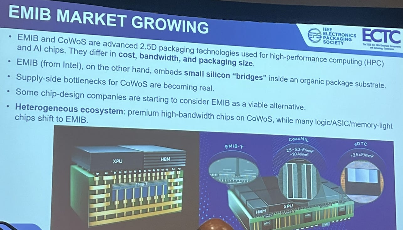
Two of the major ones high volume advanced packaging techniques are TSMC CoWoS and Intel EMIB, and is clear that Intel is becoming popular as supply chain bottlenecks for CoWoS are coming into play.
Reliability is one of the biggest concerns for engineers on the floor
Most people out there hyperfocus on the raw performance metrics of the GPUs, CPOs, the potential of hybrid bonding and glass substrates, or what Jensen is doing; they are clearly some of the flashiest subjects.
However, as GPU power increases demand more power and signal speed, these effects put more stress the package and “magnify” the existing failure mechanisms! Reliability is especially a concern as package sizes get bigger; they get heavier and introduce more points of failure.
Reliability is something historically thrown over the wall in the semiconductor industry as basically a cost center with a “line” to hit.
I was quite surprised by how much reliability was discussed among the conference among special sessions and technical sessions. There were a new notable observations amongst panelists in the special sessions:
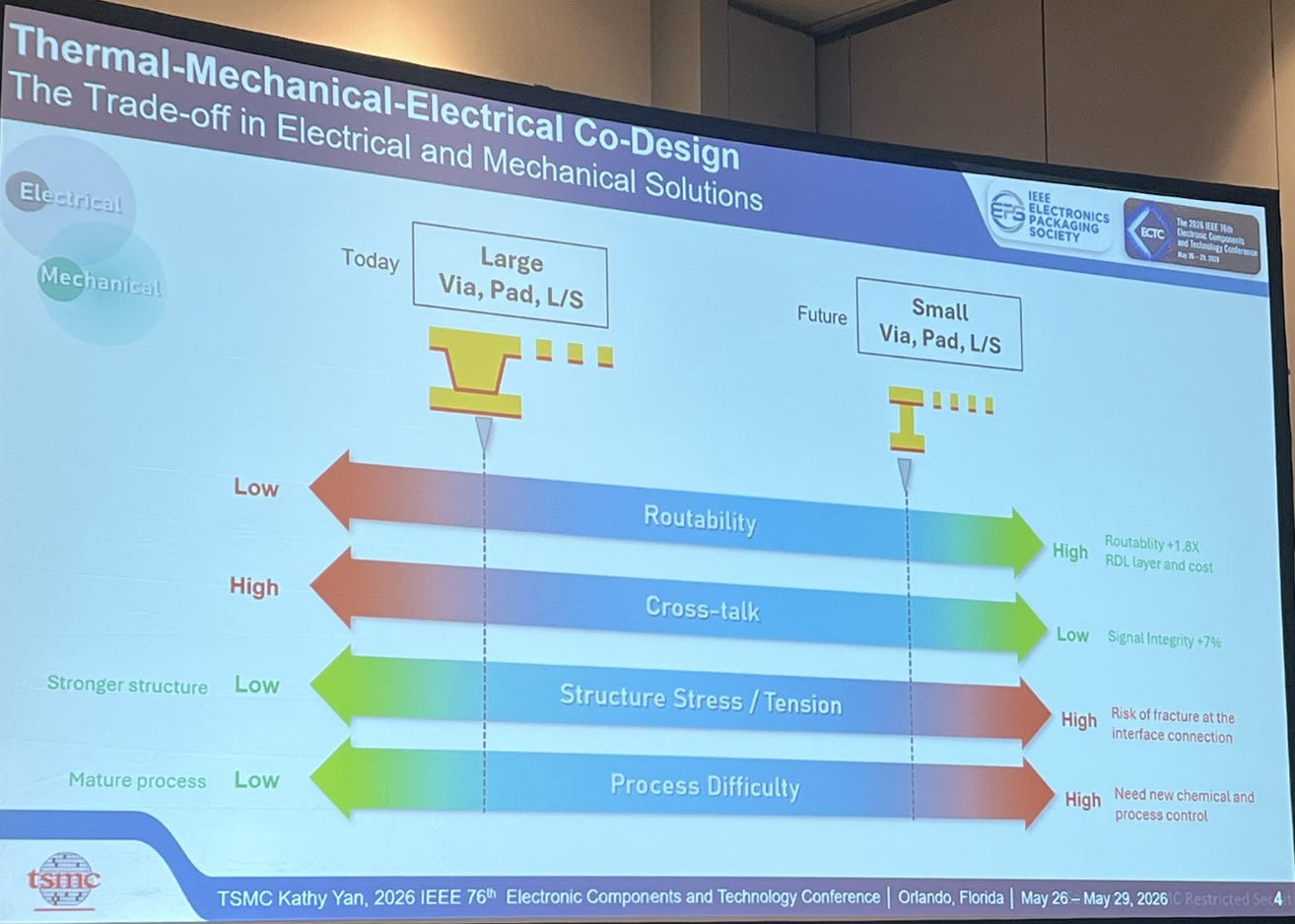
Tsun-yen Wu (in place of Kathy Yan), Department Manager at TSMC, pointed out two things:
First, there is a tradeoff between four domains in packaging:
Routability
Crosstalk (NOTE: This doesn’t appear correct; to first order, when spacing goes down, crosstalk goes up since there there is higher capacitance between the lines. However, lower line width decreases the fringing capacitance as well, so overall crosstalk depends on the dimensional scaling factors and also ground shielding used)
Structure stress/tension
Process difficulty
He also notes that many package designers tend to design their packages aggressively and not taking manufacturability into consideration early in the design, such as stacking as many vias as possible. This requires constant back and forth to ensure the package is manufacturable. This wastes communication time, especially across time zones, if a working knowledge of reliability is not known by packaging designers beforehand.
Dr. Richard Rao, Distinguished Engineer at Marvell, notes that transient switching can cause stress, and that a change from a stress strain approach to fracture mechanics approach is needed.
Gang Duan, EVP, Samsung, points out that embedding components in substrate is aggressive and can affect yield and performance
Dr. Choong Un Kim, Professor, Material Science at UT Arlington, points out that joule heating leads to local stress which leads to cracking
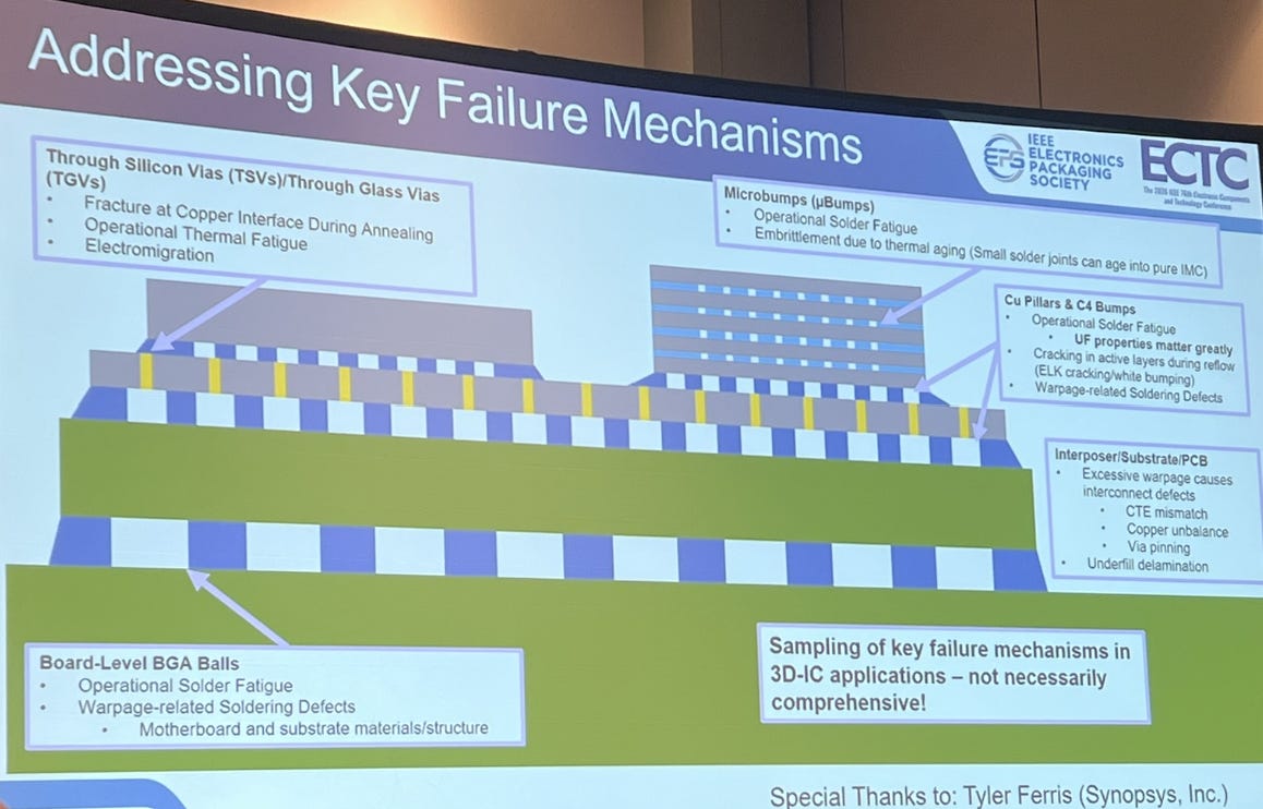
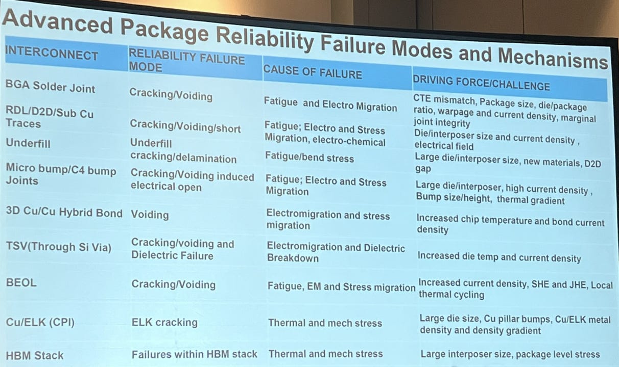
I also learned of several failure mechanisms in advanced packaging. Here are a few examples:
Much like how we personally take reliability into account when we buy a car, investors and engineers should also take reliability of systems into account. You can have a well performing part or tightly integrated system that generates buzz, but if it causes you reliability problems down the line, it might not be the best long-term solution.
I do think reliability engineering will become much more important than ever, or at the very least, a topic board level engineers MUST know as systems become more tightly integrated. I think that reliability training will go a LONG way to help minimize the cost of constant back and forth as systems become more tightly integrated.
I dive into more depth regarding the fundamental structures and physics behind these failure modes:


The Wild West of Co-packaged optics
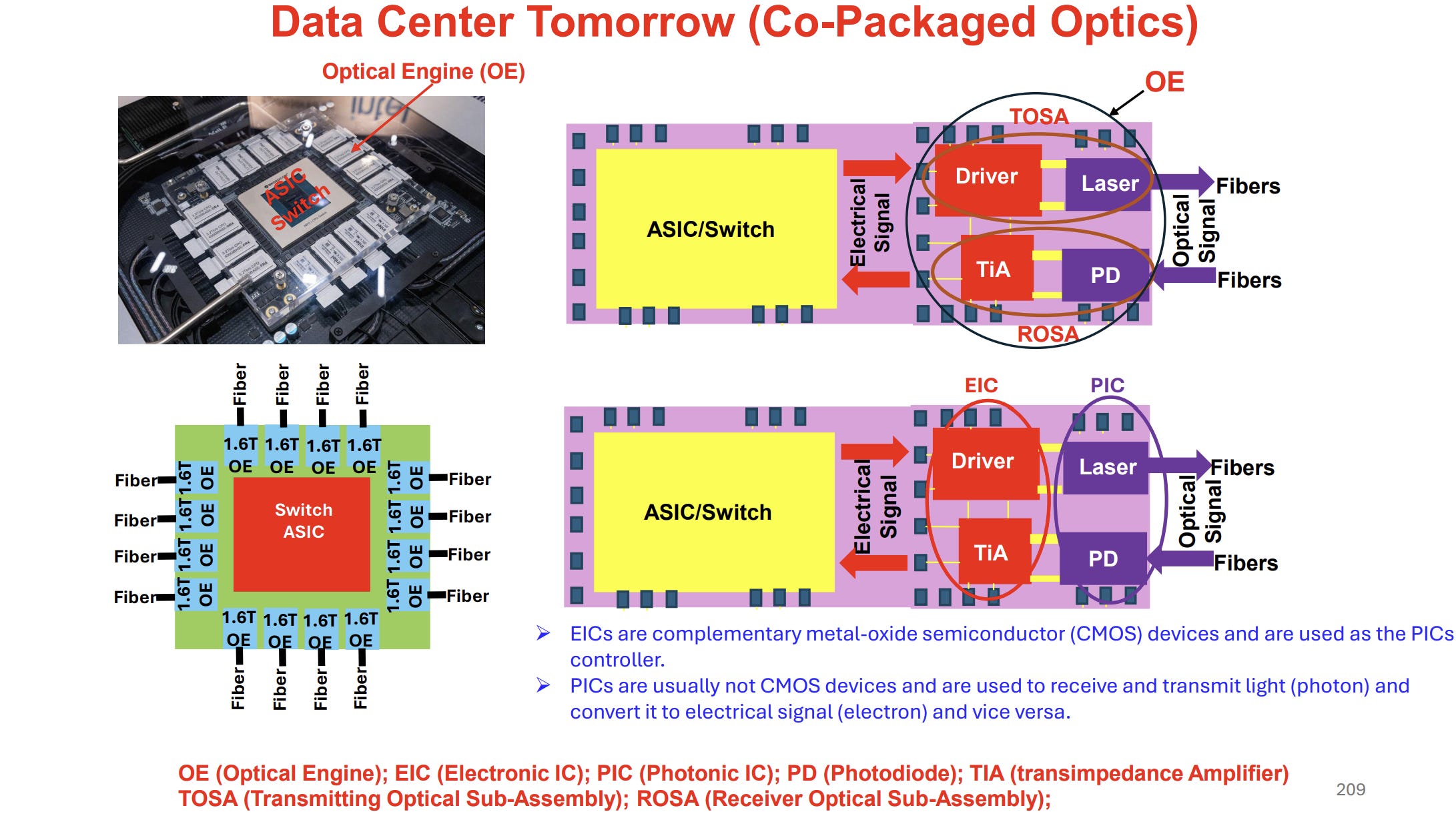
Co packaged optics is one of the hottest, yet diverse, topics of the conference. CPO consists of three major blocks:
Photonic IC (PIC) - This consists of the photonic IC such as photodiode, laser, etc.
Electrical IC (EIC) - This consists of the electrical circuits such as the transimpedance amplifier (TIA), laser driver, etc.
Application-specific IC (ASIC) Switch
There are a number of clear performance advantages of CPO that make it such an attractive option compared to pluggable transceivers, such as lower length, reducing energy to drive the signal, and lower latency. Many content creators have written exhaustively on this.
Though the physics of devices themselves can be a bit tricky, the architecture behind optical communications has a simple mental model:
You have a laser source that is routed through a PIC.
This laser is generated from a VCSEL, micro led, or other laser source.
Then, this laser source is modulated externally with either a MZM, micro-ring, or electro absorption modulator from a high frequency signal from an EIC.
This signal is sent through the optical channel at a particular “band” (850n, O,C,L), detected with a photodiode, and amplified with a trans-impedance amplifier.
I cover these in more detail in my other posts:


What makes co-packaged optics so interesting and yet confusing are the vast amount of packaging techniques involved. Each system has a own unique set of requirements for high speed data rates, system constraints, and a power/ BER link budget to handle.
For instance, here are a few options for 2D CPO structures with bridging and bumping techniques: