
A Survey of the Analog Design Process: From System Architecture to Transistor level Design
An overview of the Analog Design field, all in one post

I think of analog design as one of the more "artful" branches of electrical engineering. It requires deep intuition, careful tuning, and a sensitivity to both device-level physics and system-level performance.
This post will be a survey-level overview of each of the major abstraction levels from system architecture to transistor-level design. I want to provide a “top down” perspective of what happens at each stage of the process, so you understand how your work fits into the bigger picture.
Note: My background is deeper on the design side than dedicated system architecture and verification. I’m aiming to describe both flows at a high level and keep details intentionally light.
System architecture and modeling
Product definition translates customer/market needs into requirements (performance targets, interfaces, constraints, operating conditions) that guide architecture.
Usually, the modeling begins with an “ideal” model of a high level system. Then, levels of fidelity are added to analysis the impact on the overall system performance. This enables architectures to analyze the feasibility of a proposed topology and catch system-level sensitivities - including noise, bandwidth, and mismatch — before specifications are handed off to individual blocks.
This level of fidelity include fab-specific models:
Switching models of transistors to model anticipated loss
Non-ideal components
System-level modeling tools shine at this level. These include MATLAB/Simulink, Simscape, Verilog-AMS, and SystemVerilog. They allow you to:
Co-simulate analog and digital behaviors
Evaluate loop stability (e.g., PLLs, regulators)
Explore tradeoffs before committing to transistor-level design
Examples of such systems include:
3L Power Converter
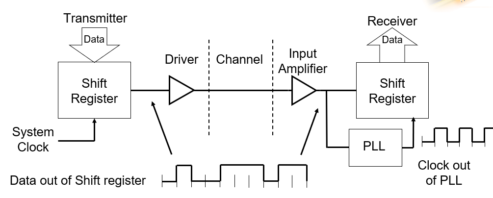
Serdes Transmitter
RFIC superheterodyne Transmitter
In summary, you want to make sure any potential issues / spec defining features are verified at the highest abstraction level with as much fidelity as possible, before passing work down as specifications and requirements to low level blocks.
This process is done while specifying blocks at a high level, such as high speed SerDes:

Design + verification: two mindsets
After system architecture, the work gets split down into two “tracks” that coordinate tightly with each other:
Block level design: implement transistors in the given process through schematic entry and layout, and make sure they are robust against PVT and aging.
Verification: try to break assumptions and validate correctness across modes/corners/interactions (often using behavioral models + mixed-level sims + regressions)
The boundary between design and verification can be a little fuzzy at times based on the complexity of the chip. Sometimes designers end up doing verification alongside design. Other items there is a dedicated verification team that adopt formal verification practices from digital like UVM.
But can’t you just simulate transistors all the time? You can, but its computationally expensive. I want to stress three points:
Transistor-level sims can be slow and unpredictable in runtime, which stretches the feedback loop.
EDA licenses are limited and expensive
Designer time is valuable and wants to focus on high level issues
In short, it is advantageous to use behavioral models if you can and simulate with Spectre when reasonable.
Behavioral modeling / co-simulation
Verification is becoming increasing important in the analog domain as well as complexity grows and simulations take longer to simulate.
Early on, teams build behavioral models of blocks to enable fast system simulation; later, those models get refined or swapped with transistor implementations as blocks mature.
Each transistor level block is “verified” by co-simulating it with behavioral models of the blocks it is supposed to interact with. The “config” view in cadence is used to swap out behavioral and transistor level views to get a feel for how blocks interact with each other. This way, one can ensure that the system behavior remains the same as transistors are slowly added.
Some teams borrow structured digital verification practices (UVM-style regressions, assertions/checkers, coverage mindset), adapted to mixed-signal.
How much behavioral modelling is needed depends on the complexity of the system:
Behavioral modelling is not always required for standalone analog blocks (like an LDO for a processor)
Behavioral modelling becomes much more important as more complexity is added onto chips, integration becomes tighter, and risk goes up of bugs.
There is an excellent paper to learn more about the design vs verification mindset called “Verification Mind Games: How to think like a verifier” [1] that I will direct you to learn more about.
It’s like the saying goes, “Trust, but verify”.
Transistor-level block design
I like to think about transistor level design as a multidimensional optimization problem. There are a dozen different paths you can go down to implement a specification, but you only have so much time.
Once block level requirements are defined:
Start with a base circuit topology or existing IP that fits the function, speed, and power envelope
Identify alternatives to topology - are there others that offer more benefits or improvements. You might look into research to identify promising ideas, or try your own.
Optimize device sizes (W/L, resistor / capacitor values) to make your design robust
One key challenge is sizing components. Digital often pushes toward minimum dimensions for speed/area, while analog frequently uses longer L in critical devices to improve matching, gain, and noise. Here are some guidelines I’ve heard:
Often 2-10X minimum L for current mirrors. Larger L values improve matching
Size W based on current handling capabilities and gm for amplifiers
Larger devices (W*L) sizes generally reduce Flicker 1/f noise
Make capacitors large enough to reduce fringing effects
Scaling parameters can be used in schematic to keep device sizes ratios of each other and avoid any unnecessarily large devices. Sometimes, performance specs can be limited by devices sizes, especially on chip capacitors, so any devices need to be added externally.
At this level you’re dealing with “second order” effects from physics and variability, such as:
Noise (thermal, shot, flicker)
Body effect
Short Channel Effects
Matching
Charge Injection
Parasitic BJTs
In addition, you need to ensure that your design is robust against process variation, aging, and non idealities. This includes:
Simulation across corners (PVT), layout parasitics, and aging (e.g., High Temperature Operating Life or HTOL) to ensure robustness
Monte Carlo to evaluate mismatch/statistical variation.
A Parasitic Extraction (PEX) at the end to verify overall circuit functionality
There are two key concepts analog people need to know: trimming, and test modes:
Trimming. Trimming is when a value of a voltage in a circuit need to be adjusted due to process variation.
Monte Carlo simulations are used to evaluate the expected trim range of a parameter
Trimming is typically implemented with digitally selectable elements (e.g., resistor strings, current/Cap arrays, DAC trims), programmed via fuses/OTP/register settings depending on product.
The level of precision depends on how precise the value need to be to drive downstream blocks or for customer specs.
Global references (bandgaps, oscillators/PLLs) are common trim targets because many downstream biases and timings depend on them.
Test Modes. Much analog functionality is hidden from the customer through “test modes”. Test modes can be thought of as “internal debugging tools” to obtain insight into what a circuit is doing at specific points. These add extra “probes” to analyze the actual circuit behavior and allows experiments to be run and observe. These are also “knobs” that you can turn to run various experiments. Typically, test mode values are written in registers that are hidden alongside the trim registers.
Adding test modes help “future proof” your design against bugs by providing more probes and knobs to turn. If there are any weird bugs, especially in new IP, you have additional insight to look at to analyze behavior and compare against simulation expectation.
Block level design is where designer intuition matters most — knowing what to tweak and when, how to recognize subtle failures, and when to trust the simulation (or not).
A map of common analog building blocks
Here are some “Textbook” circuit topologies and IP blocks that commonly appear in analog design from the low level biasing to more system oriented.
Biasing
Wide-swing cascode current mirrors
Bandgap references
Current Reference
Low Drop Out Regulator
Switches
Transmission Gate
Clocking
Ring Oscillators
Phase Locked loops
High speed
Fundamental two stage op amp
Folded cascode OTAs
High speed comparators
Gm-c Filters
High Precision:
Switched-capacitor circuits
Power amplification
Dickson Charge pumps
Gate Drivers with series inverters
ADC / DAC:
Charge Redistribution SAR ADC
Delta Sigma ADC
Support:
Common Mode feedback
Level shifters
Once blocks are defined, they can be stitched together to construct more complicated systems.
I wrote foundational primers on several of these blocks here:


Conclusion
Analog Design is such a vast, field that many designers genuinely enjoy working in, but also challenging to understand without a mental model in your head to reference into the types of activities going on around it.
In summary:
Start from the highest abstraction level
Add fidelity as you can until you need it to save simulation speed and root out problems
As more complexity is added, simulate transistor level performance using fab models against fab corners
Simulate PEX near the end
I have several block level primers above, as well as an architectural breakdown of a high speed SerDes:
References
[1] J. Montesano and M. Litterick, “Verification Mind Games: How to think like a verifier,” paper presented at DVCon (United States), Mar. 4, 2014. [Online]. Available: https://cdn.prod.website-files.com/63f4bb21bd5303fe472ad00e/649596eab21cab357fc424b7_verification_mind_games_final.pdf
Brilliant breakdown of the abstraction hierarchy. I've seen way too many teams jump straight to transistor-level sims when behavioral models couldve caught system issues way earlier. The part about fidelity management is supr valuable, avoiding expensive EDA licenses by choosing the right simulation level for each stage makes the workflow way more sustainable.