
A Masterclass on Advanced Packaging and Heterogeneous Integration
From 2D to 3.5D, a teardown of 2.5D CoWoS (TSV, RDL, Bump/pillar) and emerging trends (Glass, Panels, Bridges in Organic Substrate, and Hybrid Bonding)

Editors Note (6/22/26) - I am paywalling the last half of this post and rearranging the post outline at the beginning.
Before the paywall, I link several of my other posts in adjacent domains in power electronics, high speed communications, and signal integrity that related to packaging in some way.
In this post I’ll build intuition of the key tradeoffs and constraints surrounding advanced packaging.
I’ll define each of the classifications at a high level (from 2D to 3.5D)
Then I’ll do a breakdown of each of the key options of a TSMC 2.5D CHIP on WAFER on SUBSTRATE (CoWoS). We will examine this package architecture through the following lens:
TSV Fabrication
RDL Fabrication (with BEOL Process for Si)
Interconnect Options (C4 Bump, C2 Cu Pillar)
🔒Substrate Options
🔒Glass Substrate and the unique challenges: SeWaRe and bump reliability
🔒Panel or Wafer - Why we didn’t do panels in the first place
🔒Embedded bridge in Organic Substrate
🔒TSMC CoWoS-L vs Intel EMIB-T
🔒The Process Steps for Hybrid bonding and why it isn’t widely adopted
The reason I write this post is to establish some fundamentals of advanced packaging and communicate what a packaging engineer would like other engineers to know who are interfacing with packaging. My goal is to build on top of the knowledge on this post as well as my existing posts to be able to understand how to properly co-design electronics with the package.
Please note that I do not consider myself an expert in advanced packaging by any means. I reference John Lau’s slides from his seminar at ECTC 2026 and my overall conference experience to better understand the interactions with advanced packaging and other domains.
If you’re an expert and notice something incorrect, please reach out to me so I can have it promptly corrected.
Before I wrote this, I touched upon high level packaging issues regarding reliability, multiphysics simulation, and co-packaged optics in this post I wrote shortly after I attended ECTC 2026:

Advanced Packaging is like City Planning
Advanced Packaging is a lot like city planning:
In rural areas, houses and buildings are distributed across a large plot of land (2D)
In suburbs, houses and mid-sized buildings are bundled closer together and connected (2.1, 2.3, 2.5D)
In cities, floors are stacked both above and below with means to access them (3D, 3.3D, 3.5D)
City planning is all about managing the flow of people to and from desired destinations.
Advanced packaging follows the same logic: signals need to get to and from compute devices. However, there is an an order of magnitude difference between the dimensions of the on-chip interconnect and the PCB/package interconnect. As speed and power requirements increase, more sophisticated and elegant means of package interconnect are needed to bridge this order of magnitude difference.
Just like any building, as you start stacking floors, the structural stability needs to be considered with appropriate safety factors designed in. This logic also applies to advanced packaging as factors like reliability, thermal, and mechanical characteristics become more important.
High Level Classifications: From 2D to 3D
There are several structural variants of advanced packaging. All of these build the system on top of a build-up package substrate on top of a PCB.
Why do you need a buildup package substrate? There are a few reasons:
Package substrates help “bridge” the dimensional order-of-magnitude gap with the chip level interconnects and the board level traces. This is done through “fan out connections” where the package solder balls spread the signals out from underneath a chip.
Mechanical Buffer. The package acts as a buffer to protect the chip against stress, vibration and thermal effects. The coefficient of thermal expansion is an important consideration. We’ll see how, quite paradoxically, the low CTE of glass can have a negative impact on reliability.
Local interconnect amongst amongst chiplets. This is done through a combination of Re-distribution layers (RDLs) and Back-end-of-line (BEOL) metallization on Si Wafers
2D Integration
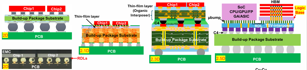
2D packaging represents the historical and architectural “baseline” packaging technology that more advanced variants build off of. In 2D we have the following classifications:
2D - the chip is bonded directly on top of a build-up package substrate.
2.1D - the RDLs (Redistribution Layers) are built as thin film layers directly on top of the organic substrate itself.
2.3D - The RDLs are fabricated separately on an organic interposer on top of a build-up package substrate. This is also known as the “hybrid approach”.
2.5D - The chips themselves sit directly on top of a massive, monolithic Silicon Core (Silicon Interposer) or a Glass Core (Glass Interposer)
In 2.1D and 2.3D, two popular materials used in the dielectric films are ABF and PID.
Ajinomoto Build-Up Film (ABF) is a resin-based epoxy film embedded with silica fillers.
ABF has exceptional mechanical stability, excellent thermal resistance, and a low Coefficient of Thermal Expansion (CTE)
Photoimageable Dielectric (PID) is almost chemically similar to photoresist; it is a liquid polymer or dry film that is chemically engineered to react directly to light.
PID can be made much finer than ABF, but is traditionally mechanically weaker than ABF.
There is a core mechanical stability vs feature size tradeoff between both films. ABF tends to be the dominant choice of packaging due to its ability to handle many metal layers.
2.1D / 2.3D are considered to be low cost alternatives to 2.5D, which is considered the standard for AI/HPC.
3D Integration
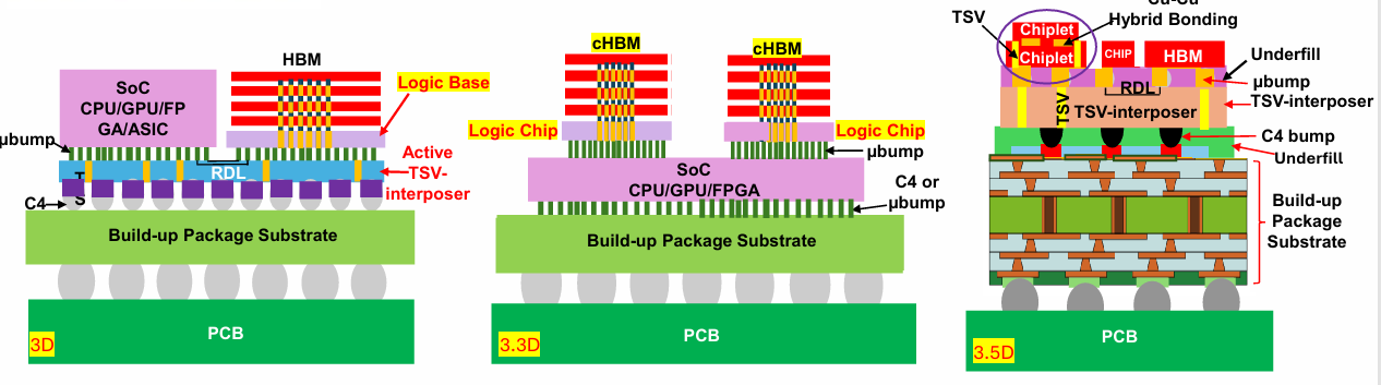
3D enables more computational density to be stacked in the vertical direction. The higher order classifications in 3D are still emerging and contested, but this is what Lau preliminarily defines:
3D - stacking chiplets directly on top of each other vertically on an active interposer (compared to 2.5D which is passive). These active interposers can contain IVRs, NoCs, BIST, or other peripheral circuitry that complement the functions of the SoC.
3.3D - consists of HBM on top of an SoC without a TSV interposer
3.5D - Involve hybrid bonding chiplets before integrating heterogeneously all components onto a single substrate.
As packages becoming increasingly integrated with the chip themselves, this leads to one of the biggest packaging challenges: whose responsibly should be for final assembly of the packaging: the fab, or the OSAT? Historically, both fab and OSAT specialized in different parts of the semiconductor production flow. The fab specialized in short pitch, finer interconnects and the OSAT specialized in higher pitch, coarser interconnects.
When hybrid technologies such as bridges and LSI in organic substrates come along, who will assume responsibility for final package integration? This is a question that is still being fiercely debated among the fab and packaging community and will be left for another time.
A Package Teardown: 2.5D
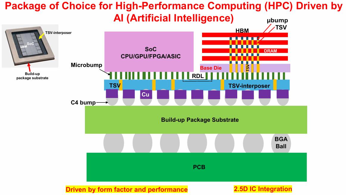
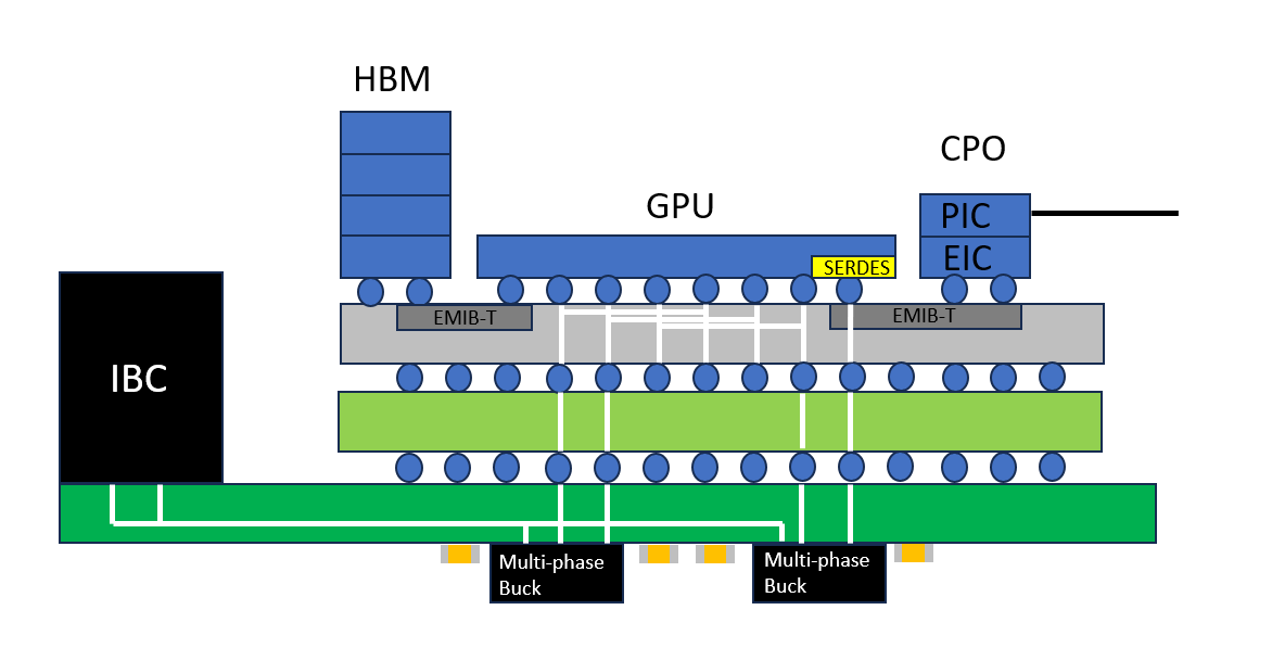
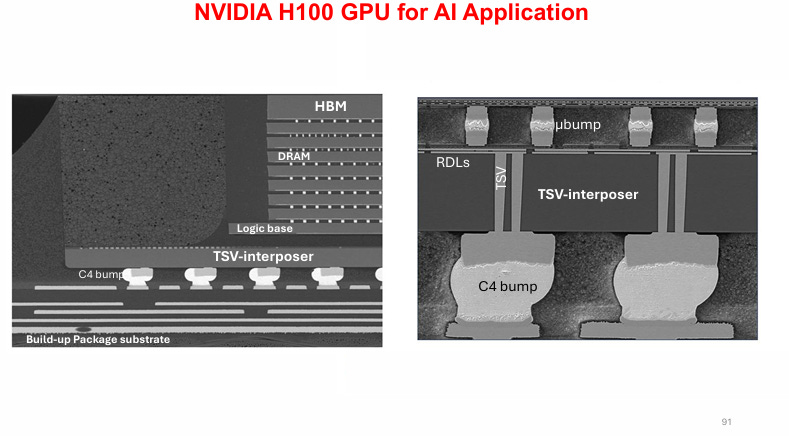
In the next section we will do a deep dive into the fabrication process of 2.5D and examine the fabrication process for each part. 2.5D is considered the package of choice for HPC due to its form factor and performance. For example, the NVIDIA H100 “Hopper” GPU uses this package and a cross section shows key features between the build-up package substrate and logic.
TSV Fabrication
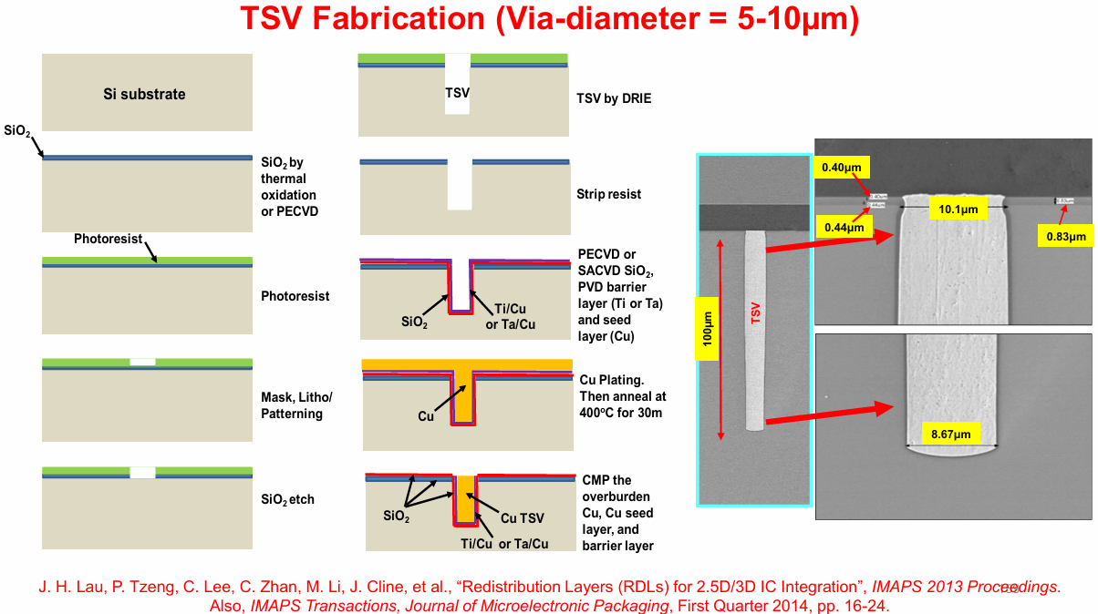
A through-silicon via (TSV) transports signals and power completely through the thick structural floor (the raw Silicon Substrate). In CoWoS, the diameter is ~ 5-10um and the pitch is ~40-50um.
Lets go through the process steps:
First, we start with standard lithography to add SiO2 on the Si surface that acts as the “hard mask” for TSV:
Deposit SiO2 by thermal oxidation of Plasma-Enhanced Chemical Vapor Deposition (PECVD)
Apply Photoresist
Pattern with lithography through a photo mask
Etch the SiO2
After the SiO2 is deposited, the via hole is formed using Deep Reactive Ion Etching (DRIE). The most commonly used process is the Bosch process.
After this hole is formed, it is filled with copper:
An SiO2 layer is added with PECVD/Sub-Atmospheric CVD to act an an electrical insulator against Si and Copper
Then, a barrier (Ti/Ta) and seed (Cu) added to prevent copper poisoning
Then, the hole is filled with copper, annealed to stabilize the grain structure, and polished with CMP.
Important thing to note: The more power TSVs you add to feed a power-hungry GPU, the more you “choke” the horizontal routing channels available for the RDLs to connect the GPU to its HBM memory.
RDL Fabrication
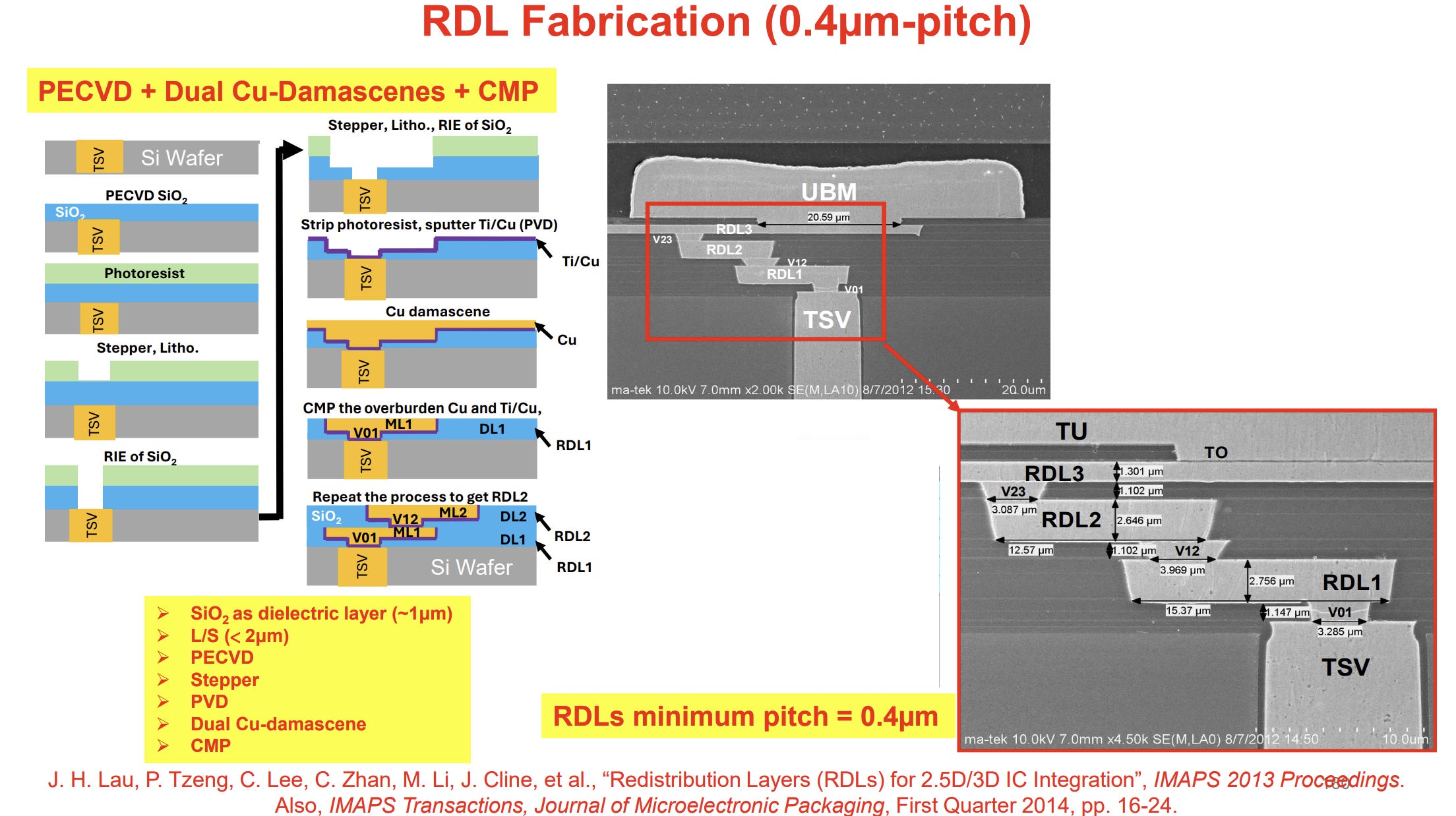
Then the RDLs are fabricated on top of the TSV using Standard BEOL Processes using dual damascene. Dual damescene refers to etching both the via and horizontal line trench before adding any metal. Heres how it works:
Form the via and M1 trenches with standard lithography. This is the same process as with TSVs: Deposit SiO2 with PECVD + photoresist on top, etch the photoresist then the oxide
Line trenches with a thin Ti/Cu seed layer with PVD
Overfill the whole trench with electroplated copper
Polish the excess copper on the surface with CMP to give you a planar surface
Compared to standard packaging methods that limit pitch to 2-5um, this method can get down to 0.4um (at the time of writing this paper).
A passive silicon interposer typically features 4 to 6 BEOL metal layers on the front-side (top), and 2 to 4 coarser packaging RDL layers on the back-side (bottom).
As more layers are added, film stress is added. With HBM4, foundries like TSMC and UMC are actively extending front-side BEOL capabilities to 8, 9, or 10 layers to accommodate the massive explosion of traces.
Interconnect Options
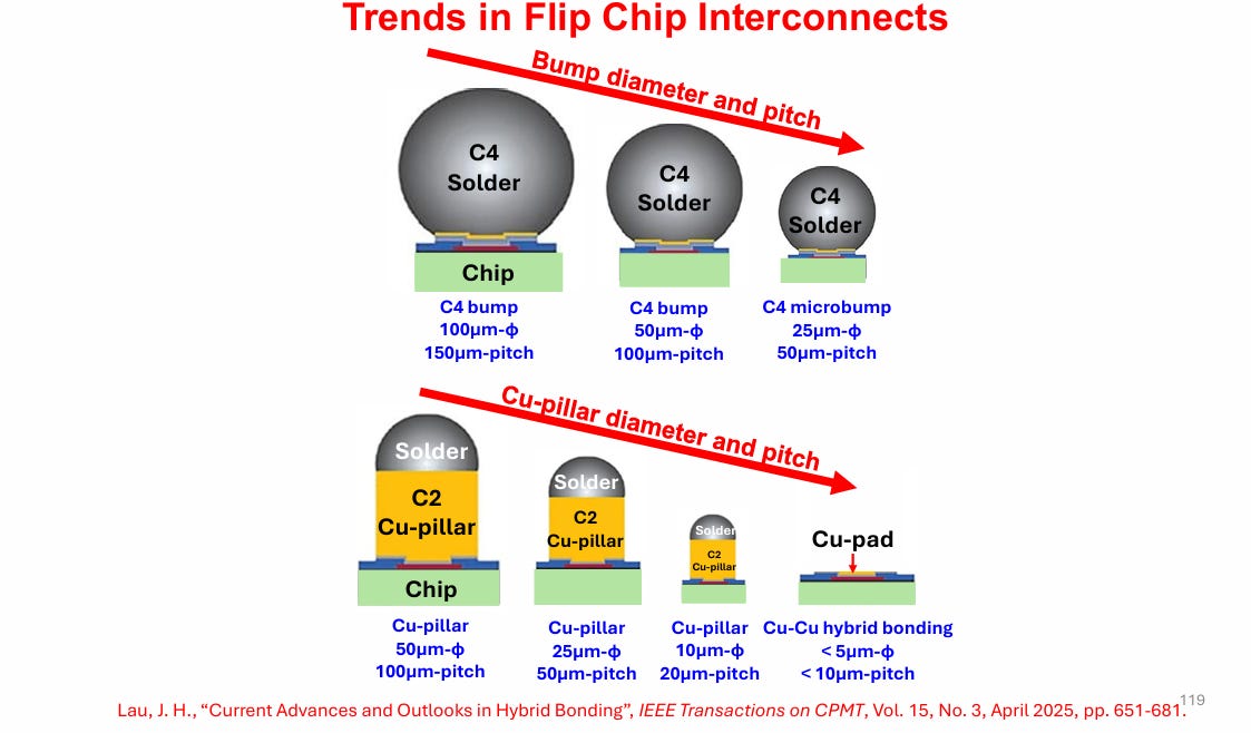
Bumps are formed by first forming an under/bump metallization with both a thin barrier layer (Titanium, tungsten, chromium) and seed layer (Copper/nickel). There are two major categories of bumps:
C4 (Controlled Collapse Chip Connection):
C4 bumps are great for macro power delivery and board-level packaging
However, the pitch of C4 bumps are limited to 50-150um because they can cause “solder bridging” if they are too close
C2 Pillar
The actual solder is just a tiny cap sitting on top of a rigid, electroplated copper that does not melt during reflow
These allow you to jam interconnects much closer together, but are much more expensive, primarily due to plating time of the Cu pillars
The other major option is Hybrid Bonding, which I’ll discuss at the end.
At higher current densities, both bump resistance and CTE affect reliability. I noticed a few posters at ECTC that demonstrate how a few small effects can magnify:
Bumps further from the neutral point of a chip experience more deformation as substrate/chip area get larger
The direction current flows into and out of the bump affects the equivalent resistance of the bump by a few percentage points
The elemental composition at the bond interface can affect current density as well.
At higher current densities, these effects can lead to localized joule heating that can create “hotspots” and can increase the probability of failures.
Substrate Options
Silicon substrates are great for fabricating the fine pitch interconnect needed in between chiplets. However, silicon substrates are running into a few problems:
They are expensive
Fabrication is limited to major IDMs
Substrates are running into photolithography reticle size limits
Silicon everywhere is frankly overkill when the fine pitched interconnect is limited to specific areas in between chips.
After the paywall, I’ll discuss the following:
Two alterative options to silicon: Glass and organic with bridges.
Panels vs wafers, and why we didn’t do panels in the first place
A brief history of hybrid bonding, the mechanism, and why its not widely adopted yet
Here are several of my other posts I’ve written that provide the technology fundamentals of power, high speed communications, and AI compute that packaging is the physical container for.


