
A Complete Deep Dive of NVIDIA DWDM Co-Packaged Optics for Scaling beyond 200Gbps
Key physics constraints and architecture challenges for scaling data rates in DWDM - ring modulator physics, clocking, CW-DFB Laser, and package integration

This post will be an advanced deep dive of a state-of-the-art co-packaged optical system based on NVIDIA’s Dense-Wave Division Multiplexing (DWDM).
This post is organized in the following sections:
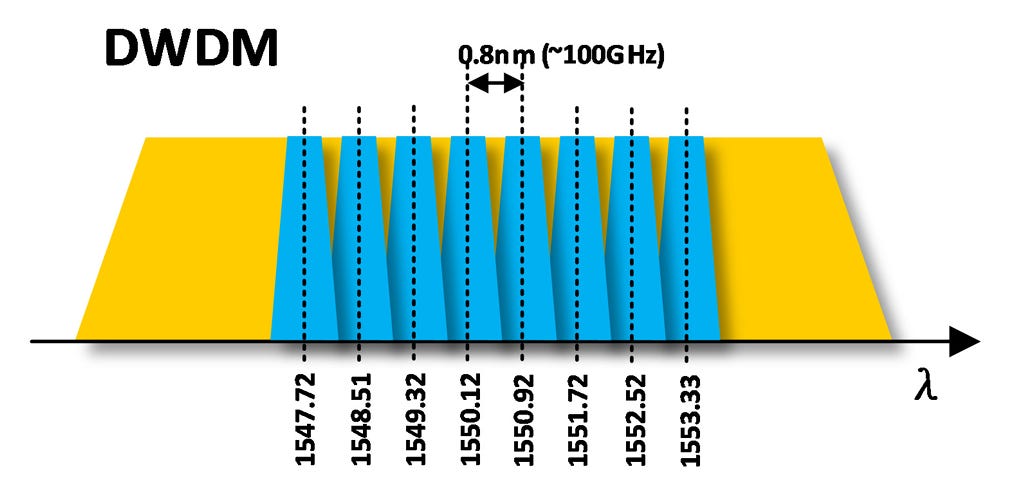
What is Dense-Wave Division Multiplexing?
A complete architecture breakdown of NVIDIAs DWDM with key physics constraints:
PIC - Ring modulator physics
Ring coupling theory - splitter and phasor theory
Key ring properties
How PN junctions shift the resonant frequency by changing the refractive index
Nonidealities - Thermal sensitivity and crosstalk
EIC - Clock forwarding and jitter analysis
Conventional clocking techniques - Forward clocking and embedded clocking
NVIDIA’s clocking architecture - half rate DWDM link architecture
🔒 A Breakdown of the DWDM CW-DFB Laser Array and performance results
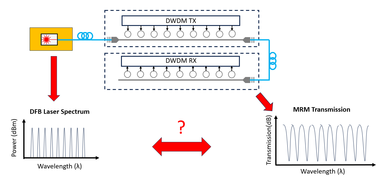
🔒 Overlay of two critical spectrums that illustrate precise alignment challenges:
🔒 NVIDIAs MRM transmission spectrum from the ISSCC paper
🔒 NVIDIAs DFB Laser Array power spectrum from the ECTC paper
🔒 A brief high-level overview of key CPO packaging features with TSMC COUPE
DWDM is fascinating because it blends together the knowledge amongst different specialties who all work together to create a successful product:
The on-chip mixed signal SerDes designers designing the high speed TX and RX circuits
The material scientists/solid state physicists quantifying the behavior of PN junctions and SiPh materials
The packaging engineers who integrate everything together
The primary sources of this post are two NVIDIA papers on the circuit architecture and packaging aspects of DWDM from conferences I attended the sessions for in-person. These are:
ISSCC 2026: “A 32Gb/s/λ 256Gb/s/Fiber Half-Rate Bandpass-Filtered Clock-Forwarding DWDM Optical Link in a 3D-Stacked 7nm EIC/65nm PIC Technology”
ECTC 2026: “Design and Packaging of a DWDM CW-DFB Laser Array for Co-Integrated Optical Interconnects”
I also integrate relevant material from relevant ISSCC forums and short courses as well.
I find that one of the best ways to learn more advanced concepts is to work backwards and figure out what simpler prerequisite concepts you need to learn first. The free half covers a huge technical breadth of material with links to several of my fundamental posts I wrote leading up to this. This way, people of all skill levels can work backwards and figure out what they need to learn to understand more complex concepts.
I want to challenge you to try to learn one new concept in depth from this post or my body of work, even if everything else doesn’t make sense.
Please note that I do not consider myself a photonics expert. I wrote this post using the sources listed above as sources-of-truth to base my commentary off of. If you’re an expert familiar with this material and notice a mistake in this post, please reach out to me so I can have this promptly corrected.
For a broad overview of optical communications, including VCSELs, optical modes, and key impairments, I recommend reading this post where I dive into these fundamentals in the free section:

What is Dense-Wave Division Multiplexing (DWDM)?
Optical interconnects in co-packaged optics help overcome the energy dissipation and frequency scaling challenges inherent in copper interconnects. Co-packaged Optics moves the optical engine as close to the chip as possible to minimize the length the electrical signal travels before being converted to the optical domain.
Optical communications enable low-energy and low-latency data transmission. However, optical communications is limited by a few constraints:
The physical edge density. The optical signals need to be propagated through waveguides into a fiber optic connector. How and where the signal flows from the laser source to the electrical devices matters a lot.
Frequency constraints of individual devices. The electrical as well as the optical bandwidths needs to be fast enough to handle the data throughputs needed.
Several companies propose solutions that push all available scaling dimensions. One of the most promising solutions to scale data speed involves densely multiplexing light signals of different wavelengths on the same waveguide.
Dense-Wave Division Multiplexing consists of individual optical channels of equally spaced wavelengths. Electrical signals are frequency multiplexed in a waveguide through a series array of micro-ring modulators. Ring modulators act like on-off switches for each of their respective channels. Ring modulators are ultra-compact, enabling many channels to be packed into a common waveguide.
Pros and Cons of DWDM
Compared to other modulation options, DWDM has several benefits:
Scalability. DWDM performance offers scaling potential with the # and size of devices.
Low latency for XSR due to no DSP
High energy efficiency
High bandwidth density
However, there are several challenges with DWDM that involve the material physics aspect of these devices:
Temperature sensitivity. Lasers and MRMs are inherently sensitive to temperature and must be well controlled
Design Complexity - DWDM moves a lot of the complexity from the electrical domain to the optical domain, and imposes unique clocking and jitter tracking challenges at high speed
Laser Integration - DWDM needs a multi-wavelength laser source that has to be brought onto the chip
Architecture Breakdown - EIC, PIC, Laser Array, and Packaging
Next I’ll discuss NVIDIAs DWDM multiplexing architecture. I’m going to describe the physics of the MRM on the PIC first to show how it works at a fundamental level. I’ll then discuss the clocking scheme of the EIC and show how the PIC requirements influence the EIC requirements.
At an architecture level, the job of an optical transceiver is to make sure that the data sent through an optical laser is received by a photodetector on the other end with acceptable BER. When selecting components, link budgeting is performed to take into account all sources of losses and optimize the performance of the entire system. I discuss link budgeting in the free section of this post:

PIC - Ring Resonator Physics
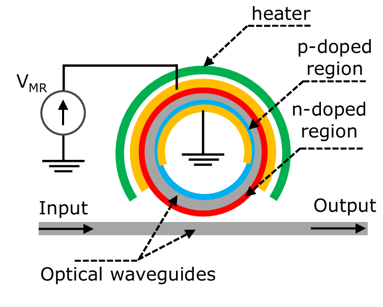
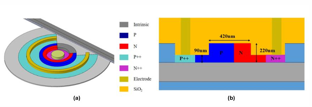
In a nutshell, microring modulators (MRM) accept or reject specific wavelengths of light going through a nearby waveguide. MRMs couple evanescently to nearby optical waveguides and act like band-stop/pass optical filters, depending on the way you look at it. Light is normally guided through an optical waveguide and passes right through, but the MRM acts like a low impedance for light at specific wavelengths.
MRMs consist of the following layers:
A circular optical waveguide (grey) that is “sandwiched” between two regions:
p-doped region (blue)
n-doped region (red)
A heater (green) that surrounds the MRM to regulate the temperature
A voltage source is attached to the n-doped region (yellow) to switch the optical signal going through the waveguide by shifting the resonant frequency over.
Lets dive into each of these elements in more detail.
Ring Coupling - the Splitter
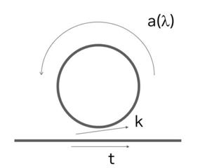
The ring can be thought of as an splitter with two input and two output terminals. . Think of the ring like a “race track” that the coupled signal enters, runs laps around, and returns back onto itself until it ultimately decays due to losses.
In this splitter network, there are two constants that define the input-output characteristics:
t is the transmission coefficient and represents how much of the signal gets through. Ideally, t should alternate between 0 and 1 at specific wavelengths.
k is the coupling coefficient and is affected by how closely spaced the ring is to the optical line.
By conservation of energy, t^2 + k^2 = 1.
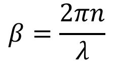
Once the optical signal enters the loop, it experiences loss and phase shift represented by a(λ). If the ring is unwound, the path of the light is represented by the phasor:

where the “a” term factors in the loss factor α and the propagation constant β that represents the wavelength-dependent phase shift:

The transmission formula is given by the ratio of the light that makes it through the optical waveguide vs the light coupled into the ring across wavelengths, which is given by:
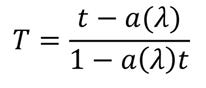
Through substitution, as well as simplifying the phasor into a cosine, we arrive the following:
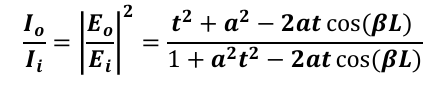
This formula lends itself to the following properties:
Rings Resonance Frequencies
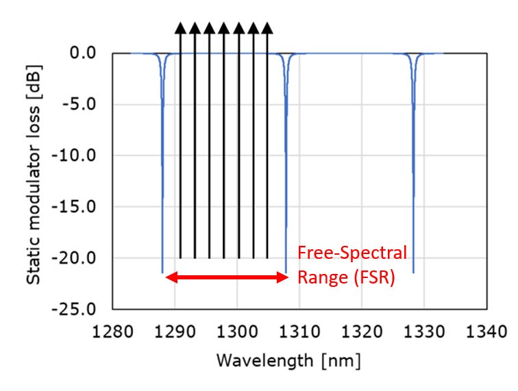
In a microring modulator, the ring resonates when the diameter is equal to an integer number of wavelengths. These wavelengths is given by
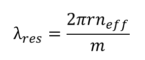
where
n_eff is the effective refractive index
m = integer modes (1,2,3…)
r = ring radius
Due to the periodic nature of the ring, the resonances are contained within a free-spectral range that limits the wavelength window signals can couple into it. Any signal outside of this window will alias into it.
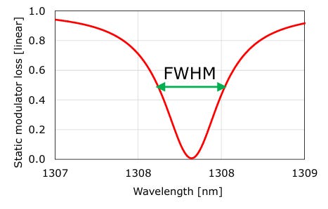
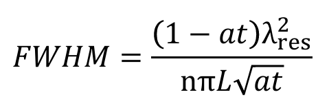
One important property of the ring is the Full Width at Half Maximum (FWHM). This is the “width” of the resonance measured at half the max power (or 3dB on a log scale) at both edges of the resonances. FWHM is a useful qualitative reference to measure how “wide” the resonance is. This is given by:
The quality (Q) factor describes how narrow the resonance width is compared to the frequency it is centered at. This is given by:
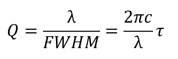
where
c is the speed of light in vacuum
τ is the cavity photon lifetime that lumps in the above parameters
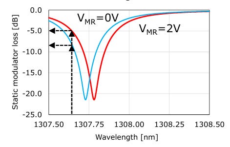
In NVIDIA’s implementation, the TX ring modulator quality factor Q is ~4.5K, and RX filter Q is ~4K.
In order to switch electrical signals into this ring, the ring bandwidth needs to be wide enough. The ring bandwidth is given by
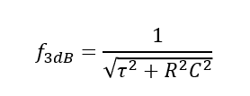
where
R is the ring junction resistance
C is the ring junction capacitance
NVIDIA switches into each ring at 32Gbps, corresponding to a switching frequency of 16GHz.
PN Junction shifts the frequency by changing the refractive index
PN junctions normally act as electronic diodes that, electrically speaking, act as one way current flow with a small built-in voltage drop (~0.7V).
In conventional PN junctions, the p side is doped with type III elements (such as boron, gallium, or indium) with free holes in the valence band, and the n side is doped with type V (such as phosphorus or arsenic) atoms with free electrons in the conduction band. When a p and n material are sandwiched together, it creates a depletion region of “built-in” electrical potential due to the flow of carriers between the materials.
However, when PN junctions are used in SiPh, we care about the solid state physics properties that affect the index of refraction. In optical, these junctions are biased in reverse bias. As more voltage is applied to the n-doped region, the depletion region widens. This lowers the carrier concentration, causing the refractive index of the silicon to spike upward. This shifts the resonant frequency and moves it just enough to allow a light source to pass through. Think of this operation like a door opening and closing really fast.
In fact, these PN structures can be altered and routed in series with the optical signal itself. Distributed PN structures are used in Mach-Zehnder modulators that modulate travelling waves along long lengths and unique structures such as p-i-n are used in electro-optic modulators. Each structural variation has their own unique characteristics and tradeoffs. I discuss these options behind the paywall in this post:
Nonidealities
I’ll discuss two nonidealities of MRMs: Thermal sensitivity and crosstalk.
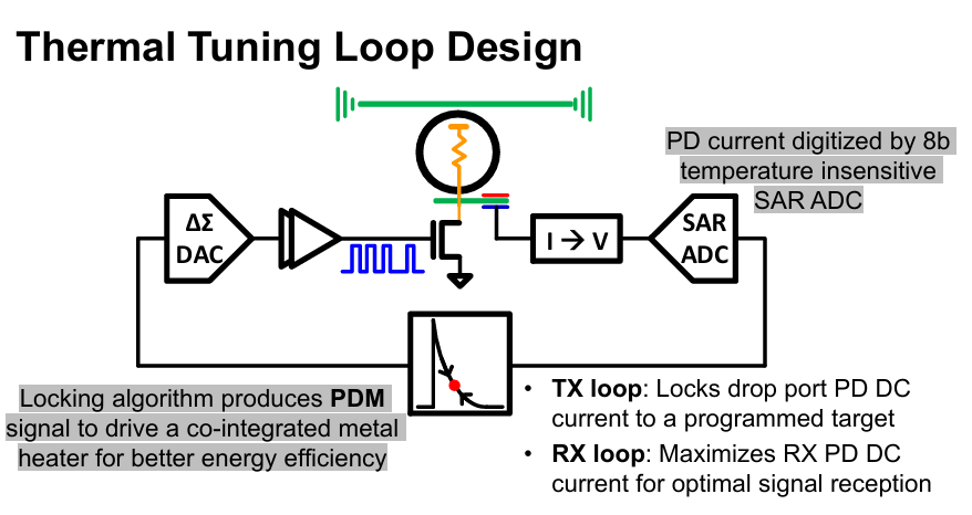
Thermal Sensitivity and Tuning Loop
Ring modulators are sensitive to temperature primarily because of the thermo-optic effect. The thermo-optic coefficient of silicon is ~1.8 x 10⁻⁴ K⁻¹ and changes in temperature affects the index of refraction.
Here, the thermal tuning loop measures the current at both TX and RX through:
A drop-port photodetector (PD) at the TX to sense how much optical power is leaking out of the ring
The TIA DC-loop at the RX
The PD current value is first digitized with an 8 bit SAR ADC, then processed digitally to produce a pulse density modulated signal to drive an integrated metal heater.
The paper doesn’t give too much detail beyond this, but I would imagine the ADC/DAC precision and loop bandwidth needs to be acceptable to correct for the expected temperature fluctuations with an acceptable wavelength error.
I dive into depth regarding the SAR ADC in this post:

Crosstalk
When multiple microrings are in close proximity to each other on the same substrate, cross talk is a key first-order phenomenon. The frequency characteristics of microrings tend to have long tails that poorly suppress sidebands and leak into other rings as well.
When deciding on what the Q factor should be, there is a tradeoff between crosstalk and the bandwidth:
A higher Q lowers crosstalk and bandwidth
A lower Q increases crosstalk and bandwidth
Modelling crosstalk is not that intuitive since there are many crosstalk paths among different rings that occur at different wavelengths.
Summary
Ring modulators appear simple at first but are highly affected by material properties and their tightly coupled nature. They are subject to device-to-device variation, so appropriate tuning circuits and control loops are needed to account for this, adding additional design complexity.
EIC - NVIDIA’s half rate DWDM link architecture
Now I will talk about the electrical side, more specifically the clocking architecture.
Of all the topics I’ve written about, I found that clocking is perhaps one of the trickiest subjects to explain in depth. As a simple analogy, think of clock synchronization like an orchestra conductor making sure all the instruments in the orchestra are in sync with minimal variation in when notes are played. There are many outside sources that can affect each individual musicians rhythm.
Each ring modulator is driven through their own SerDes electrical circuit. Compared to standalone high speed SerDes, each ring’s SerDes is slower and doesn’t have the DSP due to the XSR nature, easing some complexity. However, parallelizing 8 data lines requires synchronization and jitter control that adds additional complexity to the clock network.
Lets break down NVIDIA’s clocking architecture in more detail and see if we can make sense of this.
Conventional Clocking Techniques
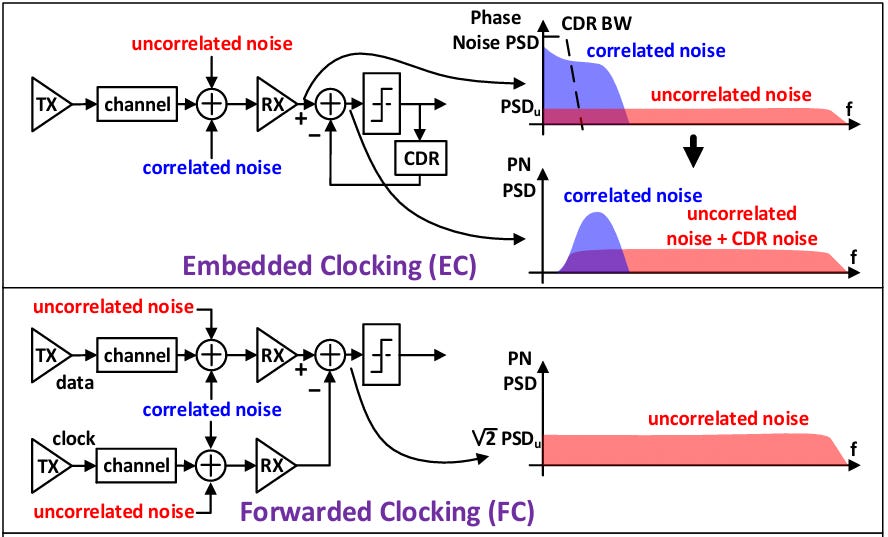
When digital data is transmitted through a channel, there needs to be some way to clock the data at the RX to recover the data. There are two conventional ways of doing this:
In a forward clocking scheme, the clock is sent alongside the data in a separate channel.
In an embedded clocking scheme, the clock is “integrated” into the data stream. The data stream is serialized in a way that ensures enough voltage transitions (edges) occur to represent the timing information. This clock is then recovered at the receiver side through a clock data recovery (CDR) circuit.
I discuss the conventional circuits used in CDR circuits (such as bang-bang phase detectors) after the paywall in the following post:

No matter which scheme is used, each channel will couple in noise that appears as clock jitter, which is a deviation of the clock edge from its ideal location. There are two types of jitter:
Correlated jitter - this is jitter that is generated from device operation such as TXPLL jitter and supply noise induced jitter. This jitter is identical lane to lane.
Uncorrelated jitter - this is jitter that is random in nature, such as thermal, flicker, shot, etc, and is mostly generated through devices. This jitter is different from lane to lane.
Jitter show up as “tails” in the frequency content of a high speed signal. If jitter is high enough, it can degrade BER from the value being outside the threshold used to read 0 or 1. I discuss more about jitter in this post:

When clocking parallel channels, it is important to track the jitter and filter out unnecessary sources of it. In general, it is easier to track correlated jitter than uncorrelated jitter, and filter out low frequency sources of jitter.
There are a few pros and cons of each scheme:
Forward clocking has excellent jitter tracking bandwidth, but requires a separate clock line. Additionally, uncorrelated jitter can accumulate.
Embedded Clocking saves on IO, but CDR circuits have the potential to be exposed to jitter beyond its limited bandwidth.
DWDM has the unique benefit of embedding the clock in as a separate wavelength along the data lines, but is does come with a a few unique challenges:
The data at the TX needs to enter the rings synchronously
When data is sent down through the optical fiber, there will be delay mismatches due to various non-idealities such as chromatic dispersion and polarization mode dispersion.
The thermal noise-induced jitter is dominated by the transimpedance amplifier (TIA) at the RX
Lets discuss what NVIDIA does to overcome these challenges.
NVIDIAs clocking architecture - half rate DWDM link architecture
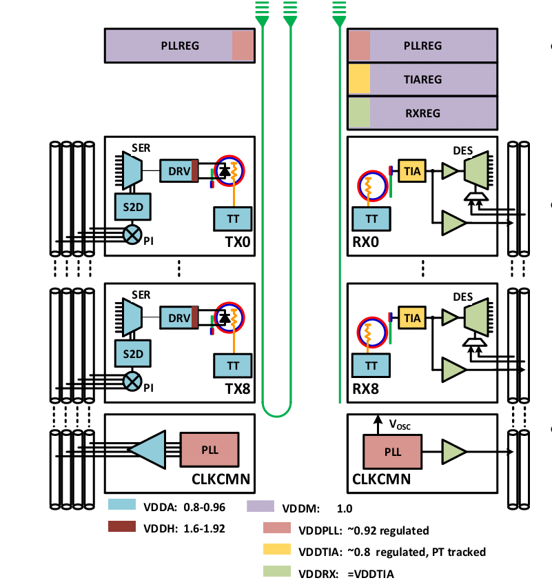
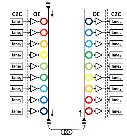
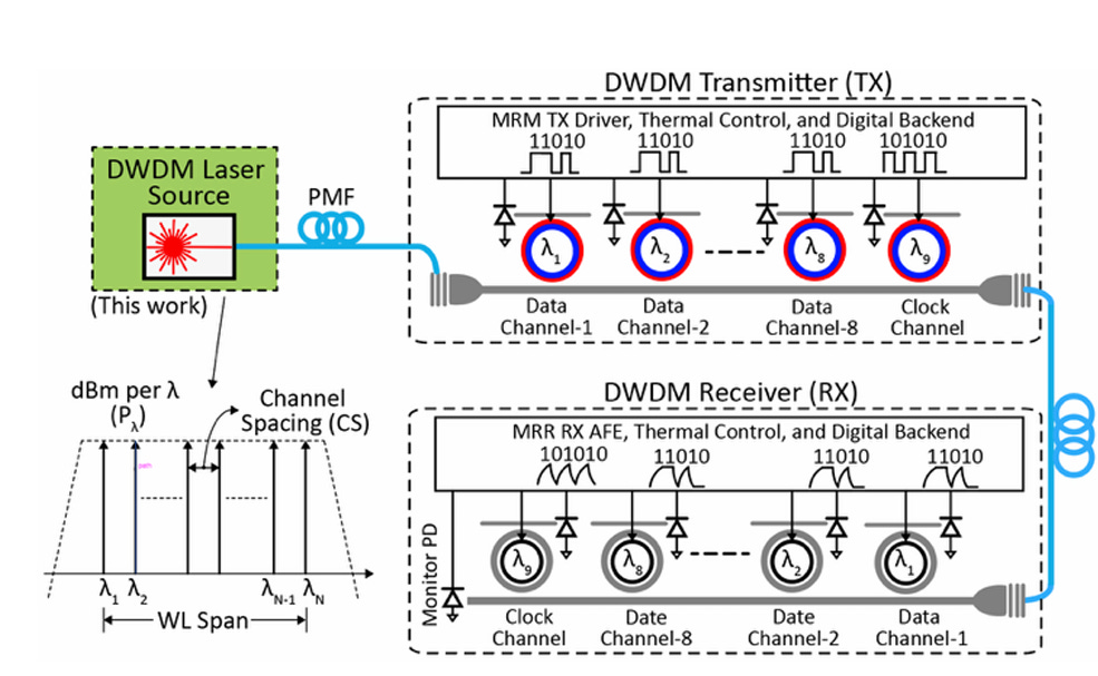
NVIDIA uses a half-rate FC DWDM link architecture that embeds the clock inline with the data. In this architecture, there are 9 rings on each of the TX and RX that combines for a total data throughput of 256Gbps:
8 rings are for data at 32Gbps each
1 ring is for FWDCLK at 16GHz
On both the TX and RX side, the signal will traverse different lengths depending on which ring it coupled into. As a result, the TX clock needs to be de-skewed to account for known path length misalignment.
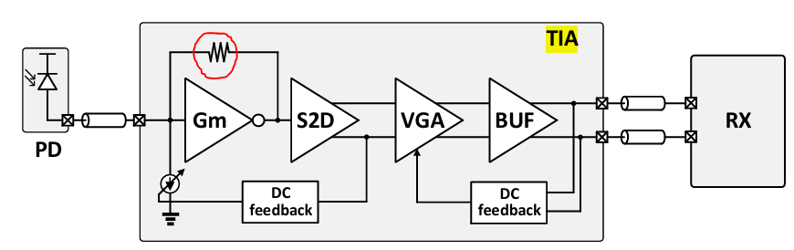
At the RX end, the transimpedance amplifier (TIA) adds a lot of thermal-noise induced uncorrelated random jitter. This TIA noise primarily comes from the feedback resistor (circled above) which is necessary to provide a low impedance input from a current sourced photodetector into the TIA.
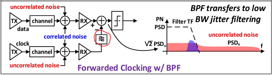
To overcome these jitter challenges, NVIDIA uses an Injection locked oscillator (ILO) - based bandpass filter to bandpass filter the clock with BW ≈ 1-2GHz. This filters out jitter beyond 1GHz to remove most of the uncorrelated jitter and tracks most of the correlated jitter.
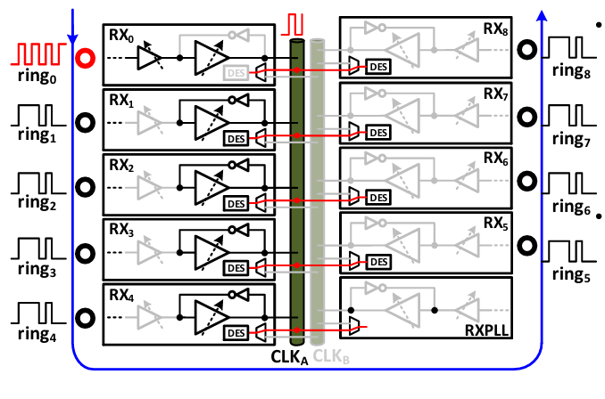
This clock is then distributed to the RX as illustrated by one example setting of the RX CLK distribution. Each RX has a local ILO that acts as another jitter filter. The clock distribution is segmented into two distinct spinal wires CLKA and CLKB that cut the capacitive load per wire in half. The RXPLL acts as a on-chip frequency synthesizer that provides the local timing reference upon startup until the system is locked to the main timing source.
I write about phase-locked loops in more depth:

DWDM Laser Source and Packaging of EIC and PIC
After the paywall, I will cover the packaging part that represents a major constraint in the physical realization of this system. I will cover the following:
A breakdown of the DWDM CW-DFB Laser Array and performance results
A brief high-level overview of key CPO packaging features with TSMC COUPE
In between these two discussions, I will overlay NVIDIAs measurements of the ring spectrum from the ISSCC paper with the DFB Laser Array from the ECTC paper, and discuss the challenges with aligning both of these. Alignment between these two spectrums is crucial across multiple devices because misaligned channels don’t transmit data.
Here are several other posts I’ve written that cover the fundamentals of advanced packaging in-depth:


